

Sterilising with far UVC
A revolutionary short-period superlattice holds the key to high-performance LEDs emitting deep within the UVC.
BY WILLIAM LEE AND LIAM ANDERSON FROM SILANNA
One of the lasting legacies of the pandemic is an increased interest in establishing efficient ways to deactivate harmful micro-organisms. Of the many options available, one that has received a tremendous amount of attention is UV sterilisation, especially in the form of the UV LED. This source offers a compact form factor, a chemical-free nature and high germicidal efficiency. However, UV LEDs come with a severe health warning: sterilisation based on most of these sources is inherently dangerous for everyday consumer use, due to the damaging effect of UVA, UVB and UVC radiation on skin and eyes.
Fortunately, there’s a solution, involving heading further into the UVC. According to a number of recent studies, when UV light is shorter than 240 nm, it is fully absorbed by our stratum corneum, the outermost layer of skin, which is 10-40 µm-thick and made up of dead cells. Due to this, light in the far UVC deactivates viruses and bacteria, but does not penetrate the shield of dead cells, so is ideal for sterilisation, because it leaves healthy cells unharmed and safe from damage.
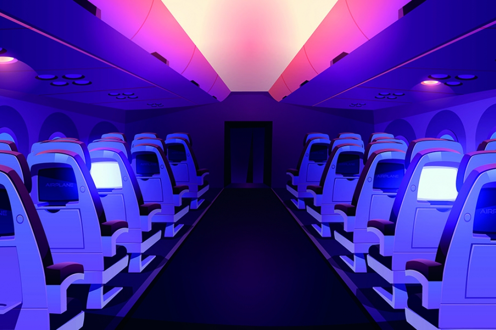
Drawing on this insight, in 2020 The American Conference of Governmental Industrial Hygienists issued a Notice of Intended Change, which proposed an increase in the exposure limit to 8 hours, for skin and eyes subjected to UV light with a wavelength less than 240 nm. This move propels far-UVC LEDs into the spotlight, as successful commercialisation of high-power sources based on this device would enable effective sterilisation tools in homes, on public transport and on planes. Implement this strategy and when the next pandemic arrives, far UVC LEDs could provide the best weapon in our defence.
Making far-UVC LEDs
Unfortunately, stretching the emission of the LED to the far-UVC is far from easy. Ever since Nobel prize winner Shuji Nakaruma generated p-type doping in GaN and demonstrated the blue LED, researchers have been developing LEDs that emit at shorter and shorter wavelengths. Realised by increasing the aluminium content in AlGaN ternary alloys, this has led to the manufacture and commercialisation of LEDs emitting in the UVA, the UVB, and more recently, the UVC. However, there is a roadblock at 260 nm, due to an inherent and unique property of the AlGaN material system that is hampering the production of high-power, efficient LEDs emitting in the far-UVC.
The inherent drawback of AlGaN comes from its bandstructure at high aluminium content. For this alloy, the valence band is split into the heavy hole, light hole, and spin split-off sub-bands, with an ordering that depends on various physical parameters of the ternary alloy. For a low aluminium content, the heavy-hole band is the top-most band, with the majority of electron-hole recombination taking place between the conduction band and the heavy-hole band. When this happens, this transition is polarised in a way that favours vertical optical emission, corresponding to transverse electric polarisation, an orientation that assists the coupling of light out of the structure.

Figure 1. When UV light shines on our skin most is absorbed while some
is reflected. Absorbed UV penetrates deep into our skin, where it is
scattered and absorbed by our cells, causing damage. However, if the
wavelength of the incident light is in the far-UVC range, it does not
penetrate past the stratum corneum, a layer of dead cells protecting
living skin cells. Consequently, UV light in this region is safe for our
skin. For similar reasons, the same wavelength range is safe for our
eyes.
Once the aluminium content in AlGaN passes a critical juncture, the ordering of the bands flips, with the top-most band becoming the spin split-off band. This band is unique – unlike the other two, its optical transition is dominated by transverse magnetic polarisation. Light with this form of polarisation has an escape cone that’s parallel to the surface. This orientation increases total internal reflection, and causes more of the light that’s generated within the structure to be trapped and unable to escape. For far-UVC LEDs emitting below 240 nm, the aluminium content is beyond this cross-over point, making the extraction of light a substantial challenge.
Unfortunately, this is not the only difficulty that’s encountered when heading deeper into the UVC. The higher bandgaps found in this domain hamper the provision of free electrons and holes, the ingredients for the light-generating recombination process. In GaN-based LEDs operating at longer wavelengths, free electrons and holes tend to be provided by n-type and p-type dopants, respectively.
As these impurities often sit at states close to the conduction band and valence band, they can generate free electrons and holes easily at room temperature. But for higher bandgaps, such as those required for the far-UVC, the two bands are so far apart that it is a challenge to find suitable impurities capable of providing states close enough to the conduction band and valence band. This fundamental limitation of wide bandgap semiconductors is another obstacle to realising efficient, far-UVC LEDs.
The strength of the superlattice
To overcome these problems and make LEDs that emit in the far-UVC, our team at Silanna of Brisbane, Australia, is pioneering the production of devices employing binary AlN/GaN short-period superlattices. With this modification, we avoid the light polarisation and doping issues that plague equivalent composition AlGaN devices. This unlocks the door to high-power far-UVC LEDs, which could be used for skin and eye-safe personal sterilisation.
Superlattices are structures with alternating materials, repeated many times. As its name suggests, in a short-period superlattice, the period of each set of repeating layers is very small – of the order of angstroms to a few nanometres. By using a short-period superlattice with layers just a few atoms thick, we alter the conduction and valence bands to such an extent that the resulting structure is essentially a new material, different from both its constituent layers and the equivalent AlGaN material. This entity, formed from a stack of hundreds of periods of AlN and GaN layers, is ideal for making a far-UVC LED, because it tackles light extraction and conductivity problems head-on.
In the active region of our device, we sandwich thin GaN ‘well’ layers between AlN ‘barrier’ layers. The quantum confinement that results creates high-energy occupied states within GaN that are dependent on its thickness.
Due to this, despite the relatively low bandgap of GaN, its thickness can be tuned to generate states emitting in the far-UVC.

Figure 2. Silanna overcomes most issues surrounding the traditional bulk
AlGaN material (left) that limits far-UVC emission by replacing this
alloy with a short-period superlattice consisting of alternative layers
of AlN and GaN, each with a thickness of the order of monolayers
(right).
What’s more, the sub-band ordering of GaN is maintained in the valence band of the short-period superlattice, due to the way that regularly incorporated gallium-atoms modify the crystal structure, no matter the thickness of the GaN well or the effective aluminium content. This means that far-UVC emission obtained from the active region of our devices is predominantly transverse electric – a vertically directed emission that can escape the structure far more easily.
Another strength of our design is that the GaN well within the short-period superlattice aids the generation of free holes and carriers. This benefit arises because the conduction bands of the wells are significantly closer to the dopant impurity levels, compared with their AlGaN counterparts. Thanks to this, our devices offer a route to ionising impurities at room temperatures, thus providing free carriers.
The other significant advantage of our architecture is that by keeping the AlN barriers thin, our repeating short-period superlattice enables quantum tunnelling through electrically active layers, improving electron and hole injection into the active area. Our wells offer a significantly improved recombination efficiency, because they are thin enough to significantly increase carrier overlap in the emitting areas, by reducing the quantum-confined Stark effect despite the strongly polarised lattice of GaN and AlN.
Merits of MBE
Due to the precise thickness control required for making a III-N short-period superlattice, we do not produce our devices by MOCVD, the most common approach for making GaN-based LEDs. Instead, we use MBE, a kinetic non-equilibrium process that’s frequently used at the forefront of material research. With this form of epitaxy we can realise precise thickness control and produce high-quality short-period superlattices featuring barriers with monolayer thickness and wells with abrupt interfaces.
Our far-UVC LEDs are produced using the only production-grade nitride MBE system in the southern hemisphere. With this tool we can deposit highly uniform short-period superlattices on 150 mm sapphire substrates with a thickness accuracy within a single layer of ±0.2 monolayers.
According to X-ray diffraction ω-2θ scans, our short-period superlattices are of excellent quality. This is evident by the number of characteristic satellite peaks, as well as their intensity and sharpness. Confirming the structural perfection of our epilayers is transmission electron microscopy, which reveals the abrupt interface of alternating layers of AlN and GaN.

Figure 3. (a) The valence band ordering of Al0.8Ga0.2N, showing that the
spin split-off (CH) band is at the top of valence band at the gamma
point (left). The CH band promotes emission with an optical dipole that
is parallel to the surface, resulting in reduced centre irradiance and
poor light extraction from the top/bottom surface (right). (b) The
valence band ordering of a 1ML:4ML GaN/AlN short-period superlattice,
which has an equivalent aluminium content of Al0.8Ga0.2N. The effect of
the short-period superlattice is to put the heavy hole (HH) and light
hole (LH) band above the CH band, resulting in emission with optical
dipoles perpendicular to the surface. This allows a strong centre
irradiance to be maintained, with most of the emitted light able to
escape the structure.
As expected, and unlike AlGaN, our short-period superlattice is capable of high n-type conductivity, using silicon as a dopant. Resistivity measurements reveal that for a structure with an aluminium content equivalent to Al0.8Ga0.2N, resistivity is just 0.015 Ω cm. This value is significantly lower than that reported by others for Al0.8Ga0.2N, underscoring the doping benefits of our short-period superlattice technology.
To fully exploit the merits of our short-period superlattice, this structure features in almost the entirety of our LED. Producing such a device poses unique challenges, including those related to carrier transport. The ease with which carriers quantum tunnel through our short-period superlattice is both a blessing and a curse: it enhances carrier injection into the active region, but also promotes carrier overshoot into the doping layers, cutting recombination efficiency. However, it is possible to balance carrier injection and carrier overshoot by carefully designing the electron-blocking layer, which sits between the active layer and the p-layer. In our short-period superlattice structures we can enjoy a similar outcome by adjusting the thicknesses of barrier and well, to tune the degree of quantum tunnelling through the device.
Before we optimised our device, we produced a benchmark with an arbitrary short-period superlattice that had been shown to emit at the correct wavelength. Driven at 8.5 V, this far-UVC LED emitted 0.03 mW at 20 mA.

Figure 4. (a) Transmission electron microscopy image of a typical
short-period superlattice, showing layers of AlN (dark) and GaN
(bright). This atomic scale image shows that the constituent layers are
distinct, with well-defined interfaces, confirming the high quality of
the short-period superlattice. (b) X-ray diffraction ω-2θ scan of a
typical short-period superlattice, showing a wealth of satellite peaks.
The observation of high-order satellite peaks for multiple reflections
(colour coded) underscores the extremely high quality short-period
superlattice produced by the Silanna process.
We have optimised our device structure by: increasing the barrier width in the active layer, so that this strikes a balance between electron injection and overshooting into non-active regions; using an n-doped layer with barrier and well-widths optimised to strike a balance between carrier transport and optical properties; and employing a short-period superlattice with an optimised grading profile as an additional electron-blocking layer. These improvements have increased the output power of our die by almost 20-fold while maintaining a low drive voltage. Our latest far-UVC 235 nm sources typically operate below 7 V at 20 mA, which is lower than comparable products on the market. For this drive current, output power is typically 0.7-0.8 mW, higher than most commercially available far-UVC LEDs. Through further improvements to device design and process, we have even demonstrated an output power of 7 mW at 200 mA, for a 235 nm LED at the wafer level. This is the highest value ever reported in this wavelength range, realised for a device operating at just under 8 V.

Figure 5. Heterostructure for Silanna LEDs, utilising the short-period
superlattice through almost the entirety of the device stack.
The added bonus of our uniform 150 mm wafer process is that we produce many die within a single run. Right now, we can make over 9,000 die that pass our product specs from a single wafer. Note that every one of them has a wavelength within a few nanometres of our target.
One of the merits of producing a large number of die is that it allows us to properly evaluate product reliability. This assessment shows that our far-UVC LEDs are more reliable than most on the market. Results from more than 160 die show an L70 lifetime of over 2000 hours, using TM-21 valuation. A significantly longer lifetime is possible after burn-in.
Currently, we have established two product lines based on our short-period superlattice technology – the far-UVC 235 nm SF1 series we demonstrated here, and the deep-UVC 255 nm SN3 series. This portfolio provides the perfect solution for various deep and far-UV use cases, such as water sterilisation, sensing, and instrumentation applications.

Figure 6. (a) Electroluminescence spectrum of Silanna far-UVC LEDs,
showing an over-20-times improvement in emission output after
optimisation of the short-period superlattice. The inset shows the
effect of optimisation on the electrical properties of the LED,
including a reduction in the operating voltage at 200 mA to below 7.5 V.
(b) Wafer-level plots of output power versus current, and external
quantum efficiency versus current, of one of Silanna’s best dies
emitting at 235 nm. Measurements show a power of over 7 mW at 200 mA,
and a maximum external quantum efficiency of over 0.8 percent.
However, the promise of the short-period superlattice extends beyond just these opportunities. Due to the unique nature of this technology, it is easy for us to produce LEDs of any wavelength in the deep to far-UVC, using the same process and a simple adjustment in thickness. This allows us to target new applications requiring UV emitters at wavelengths currently unavailable, such as those within the 240-250 nm range.

Figure 7. (a) Silanna’s 150 mm wafers are fully utilised, with over
10,000 die fabricated from each wafer. (b) The uniformity of the 150 mm
MBE process ensures that the majority of die produced within one wafer
run have very similar properties. For example, the wavelength variation
is typically only a few nanometres across the majority of the 150 mm
wafer.
In the near future, we will focus on further optimisation and improvement to the two existing wavelength ranges, and push the boundaries to realise even higher output powers in the far-UVC region below 230 nm. Supporting such efforts is our recently commissioned brand-new production facility in Brisbane, Australia, featuring state-of-the-art equipment and facilities – this will aid us in our goals of developing new technologies and processes. Further foundations supporting tomorrow’s success are our ISO90001 certification and our long history in electronics production and manufacturing. Thanks to all these attributes, we are perfectly positioned to turn our next technology breakthrough into brilliant products for our customers.

Figure 8. As per the IES standard TM-21, the L70 lifetime of Silanna’s product has been evaluated using an average normalised output value, observed over 78 samples. The resulting L70 is 2500 hours with a similar B50L70 value. It is expected that the die lifetime can be further extended using a pre burn-in procedure.
Further reading
ACGIH 2021 TLVs and BEIs: Based on the Documentation of the Threshold Limit Values for Chemical and Physical Agents & Biological Exposure Indices; American Conference of Governmental Industrial Hygienists: Cincinnati, OH, 2021


