
TiO2 enhances Ga2O3 diodes
Thanks to a high dielectric constant and a favourable band alignment, TiO2 enables b-Ga2O3 diodes to realise a higher breakdown and a lower turn-on voltage
A key challenge facing designers of any power device is to ensure low losses under both forward and reverse bias. While success on these two fronts has proved particularly challenging with b-Ga2O3 diodes, progress may be realised by introducing a high-k TiO2 interlayer, according to a US team led by engineers at the Air Force Research Laboratory (AFRL).
This partnership, which includes researchers at University of California, Santa Barbara, and APEX Microdevices, has recently reported that inserting a TiO2 interlayer trims the turn-on voltage and leakage current of the Ga2O3 diode, and increases its breakdown voltage.
“Time will tell whether this is the most promising topology,” says team spokesman Nolan Hendricks from ARFL. “But, at the very least, this topology with TiO2 can be combined with other diode designs like junction-barrier-Schottky or trench-MOS Schottky diodes to unlock the full potential of Ga2O3.”
Hendricks and his co-workers are by no means the first team to investigate new device architectures for improving the performance of Ga2O3 power diodes.
A number of designs have already been reported that succeed in reducing the off-state current density. They include: trench-based structures, which are hampered by an increase in the specific on-resistance; devices with high Schottky barrier contacts, which cut leakage but increase the turn-on voltage; and diodes with p-n junctions that increase the barrier height, leading to higher on-state losses.
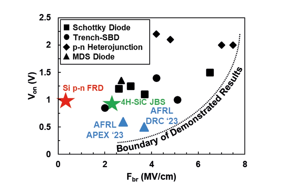
Offering more promise, argues Hendricks, is the metal/BaTiO3/Ga2O3 structure pioneered by the team at Ohio State University, led by Zhanbo Xia and Siddharth Rajan.
“The metal/BaTiO3/Ga2O3 structure gave a very large turn-on voltage due to a slightly positive conduction band offset, but the fundamental concept they conceived of was quite promising,” says Hendricks. “When we saw that TiO2 was also high k but should theoretically have a negative band offset to Ga2O3, we got to work on implementing it in the metal-dielectric-semiconductor structure. The results have been great.”
TiO2 has a dielectric constant of 30-160 and a conduction band edge that is around 0.3 eV lower than b-Ga2O3. These characteristics promise a reduced leakage at reverse bias, due to improved blocking of tunnelling electrons, and no impairment to forward conduction, thanks to the band profile.
To determine whether TiO2 could fulfil its promise, Hendricks and co-workers fabricated a conventional b-Ga2O3 Schottky barrier diode and a Pt/TiO2/Ga2O3diode in parallel. These devices were formed from adjacent die on a wafer containing a 13 mm-thick, silicon-doped b-Ga2O3 layer grown by HVPE on a tin-doped native substrate. Plasma-enhanced atomic layer deposition added a 4.3 nm layer of TiO2.
Measurements on both types of diode, featuring edge passivation through the deposition of SiO2, revealed that inserting TiO2 lowered the turn-on voltage from 0.88 V to 0.59 V and increased the breakdown voltage from 548 V to 1380 V, corresponding to an increase in the breakdown field from 1.8 MV cm-1 to 2.8 MV cm-1.
Hendricks regards these results as “very exciting”, arguing that the breakdown field for the team’s Pt/TiO2/Ga2O3 diodes exceeds the limit of 4H-SiC in a planar topology, which also has a higher turn-on voltage.
Note that these results were realised without edge termination. This is now being introduced, with the team considering a range of field management structures that allow low resistive losses and a low turn-on loss. “We have already demonstrated an early advance in that area, pushing the breakdown field up to 3.7 MV/cm through p-NiO guard rings, which we shared at Device Research Conference 2023,” says Hendricks, who is now hoping to make additional progress in increasing the breakdown field while realising a low forward voltage.
Pictured above: the results presented in the journal Applied Physics Express and at this year’s Device Research Conference showcase the potential of Pt/TiO2/Ga2O3 diodes
Reference
N. Hendricks et. al. Appl. Phys Express 16 071002 (2023)


