Multiple opportunities for long-wavelength VCSELs
Propelling VCSEL emission further into the infra-red with InP-based
designs creates lucrative opportunities in data transmission and sensing
markets.
BY CHRISTIAN NEUMEYR FROM VERTILAS
Two decades of substantial sales have helped to establish the VCSEL as a mainstream laser technology. Initial success came from short-reach optical communication, with devices emitting at 850 nm enjoying widespread deployment in data centres. And more recently, 3D sensing has become the ultimate killer application for VCSELs, such as 940 nm variants that enable facial recognition in many models of smartphones.
Additional opportunities are now emerging further into the infra-red, particular for wavelengths between 1.3 µm and 2.3 µm, where VCSELs can offer an attractive alternative to edge-emitting lasers. VCSELs that operate in this spectral range can provide eye-safe sources for sensing, and find applications in optical networks, where they draw far less power than the incumbents, enabling high-density multi-channel interconnects.
At Vertilas of Garching, Germany, we are ideally placed to capitalise on these new opportunities. We have more than 20 years of experience in producing lasers, including tremendous expertise in the manufacture of InP-based VCSELs that emit at longer wavelengths within the near infra-red.
Following the launch of our company in 2001, we enjoyed initial commercial success from a portfolio of VCSELs for gas sensing, with products covering more than 15 wavelengths from 1.3 µm to 2.3 µm. Since then we have expanded our horizons. More recent breakthroughs include: the development of the fastest 1.3 µm and 1.55 µm single-mode lasers for optical data transmission, delivering 40 Gbit/s data rates in 2017 and 2014, respectively; and the launch of 1.3 µm 2D VCSEL arrays for 3D sensing applications in 2022 (see “Key technology milestones of Vertilas InP VCSELs” for a more detailed account of our triumphs).
The VCSELs and VCSEL arrays that we produce are well suited for applications in data communications and metro networks, which are built around 10, 100, and 400 Gbit/s modules and interconnects. New data centres and infrastructure for fast-growing cloud applications are increasingly based on single-mode fibre transmission, so there is a significant opportunity for sales of energy-efficient long-wavelength sources that meet this criterion.
Our 10 and 40 Gbit/s VCSELs are strong contenders in this market, combining a single-mode output with ultra-low electrical power consumption – it is less than 20 mW. As VCSELs are also renowned for their small die size and integration capabilities, our devices are ideal for multi-channel grey or multi-colour dense-wavelength-division multiplexing optical interconnects and modules.
As well as eye-safety, our long wavelength 2D VCSEL arrays have additional merits for serving 3D sensing and illumination markets. Whether deployed in robotics or autonomous vehicles, face and gesture recognitions systems or automotive lidar, our sources can help to prevent sunlight interference while ensuring cost-effective small-form-factor packaging.
Figure 1. Vertilas’ InP BTJ design and BTJ defined active area DBTJ.
InP: The essential ingredient
Our VCSELs are notably different from their short-wavelength cousins, which have enjoyed so much success in data centres and facial recognition. Those devices are based on GaAs, a material system that limits the emission wavelength to around 1 µm. Introducing novel alloys, such as the dilute nitride GaInNAs, can allow the output to extend further into the infra-red, with the ceiling raised to 1.3 µm. But there needs to be a radical departure from the norm to span the domain from 1.3 µm to 2 µm, with a switch from GaAs to InP providing by far the best option.
To make this transition, we have addressed a number of key technological challenges. One downside of the move to longer wavelengths is that the distributed Bragg reflector, which requires exceptional reflectivity, is hampered by a lower refractive index contrast between suitable materials and a higher thermal resistance.
Additional challenges include developing an approach to implement reliable, defined current confinement, and to ensure an effective current flow from the active area to the heat sink. Once we addressed these design-related issues, we still had to: demonstrate high-performance, single-mode laser characteristics; realise singlets and 1D and 2D arrays; introduce cost-effective production, assembly and test procedures; and make sure that our VCSELs offered long-term reliability and adhered to industry qualifications, such as those of Telcordia.
Taking on these challenges led us to create a novel laser design. By implementing a new concept, and integrating innovative device functions, we have realised VCSELs that can perform at up to 90°C.
Initially, we focused on the thermal management of our VCSEL and the design of its active region. While targeting these objectives, we had in mind the need to develop a device with low power dissipation, high performance and long-term reliability. The design that resulted is shown in Figure 1.
If we were to use epitaxial DBRs for the top and bottom mirrors, as is the case with a GaAs VCSEL, this would result in a very ‘thick’ device. So we combine one epitaxial DBR with a dielectric variant. The epitaxial DBR, which is lattice-matched to the InP substrate, consists of a high number of InAlAs/InGaAlAs mirror pairs, leading to a relatively high thermal resistance. Depending on the target wavelength, we use between 30 and 40 mirror pairs to realise a DBR with a thickness of around 8 µm and a reflectivity of around 99.6 percent. In comparison, GaAs/AlAs DBRs realise the same reflectivity with less than 20 mirror pairs. However, despite the increased effort and the thicker DBRs, it is acceptable to pursue this approach.
The same cannot be said for the bottom DBR. This mirror requires a reflectivity of 99.9 percent, leading to a total device thickness of potentially 20 µm or more. As well as high production costs stemming from the long epitaxial growth time, such a device would suffer from a compromised thermal performance, due to its high thermal resistance. The hottest spot within the VCSEL is the active region, and it’s essential to have a very effective heat flow from there to a heat sink, to prevent the device from overheating. If the VCSEL’s operating temperature is too high, this results in inefficient conversion of electrical energy to photons.
Our solution is to use dielectric materials for the bottom mirror. Options for this include the pairing of AlF3 and ZnS, which have a very high step in refractive index. With this combination we form a bottom mirror with only 3.5 mirror pairs. To ensure excellent thermal management, we also introduce a very effective heat sink structure, created by deploying a plated gold substrate at the bottom of the wafer (and VCSEL). Thanks to the short distance between the active region and heat sink, the heat that’s generated within the quantum wells flows effectively to the heat sink, ensuring excellent thermal performance for the VCSEL.
Figure 2. Optical spectrum of a multi-mode VCSEL and output
power of the Vertilas single-mode and multi-mode (8 mm) InP VCSELs.
Last but not least, our long-wavelength VCSELs feature a buried tunnel junction (BTJ). This addition enables sufficient current confinement for realising a high energy density in the active region, which consists of a quaternary InGaAlAs material structure that features around five quantum wells.
There is much to be said for using a BJT, rather than an oxide, the common choice for carrier confinement in GaAs VCSELs. One of the strengths of the BJT is that it can be formed after epitaxial growth by means of dry etching, so there’s no need for an oxidation step that threatens to degrade the aluminium-containing active region. While there’s a need for high-doping to form a tunnel junction, this is well within the capabilities of MBE. And as the BTJ is formed with a well-defined dry etching process step, there’s great control over the dimensions of the active area and thus the optical power capabilities of the device (see Figure 2). If high-powers are required, and multi-modes are acceptable, the diameter of the BJT can reach up to 12 µm; but if single mode is essential, the diameter of this junction is typically just 5 or 6 µm.
We produce both single-mode and multi-mode VCSELs. The former results from an optimised waveguide design and judicious selection of the BTJ diameter. Our 1.3 µm InP-based VCSELs provide a side-mode suppression ratio of more than 40 dB (see Figure 3).
Figure 3. InP BCB VCSEL (top view).
Delivering data
The key requirements for VCSELs for optical data communication are: a high bandwidth, evaluated in terms of the -3dB point of the S-parameter S21; a low power dissipation; a low threshold current; and sufficient optical power at temperatures of up to 90 °C. We have fulfilled all of these requirements by refining the design of our device. High performance comes from using a threshold current of around just 1 mA and trimming the device’s intrinsic parasitics. They are lowered by dry etching a semiconductor mesa for each VCSEL on the wafer. Etching reduces the amount of semiconductor material and minimises the capacitance of the device structure. After this step, we fill the voids with benzo-cyclo-butene (BCB), a polymer with low dielectric characteristics.
Figure 4. Single-mode VCSEL optical spectrum .
With this approach we produce InP VCSELs with a S21 3dB bandwidth of up to 12 GHz, which is more than sufficient for 10 Gbit/s applications. These devices, containing BCB and having a 1.3 µm-matched cavity, provide excellent performance at temperatures of up to 90 °C. Evaluating their capability for optical data transmission with the commonly used ‘eye measurement’, formed by sampling the output of a laser that’s directly modulated with a pseudo-bit-rate sequence, reveals an eye mask margin of 42 percent when transmitting data at 10.3 Gbit/s (see Figure 5).
Even higher levels of performance are realised by shortening the length of the cavity. While doing so, we have reduced the photon lifetime by replacing the top epitaxial DBR with a thinner dielectric DBR. These changes, which have led to a reduction in resonator length by around 30 percent, have enabled an increase in the S21 bandwidth to 18 GHz, and a 26 percent eye-mask margin for a data rate of 25 Gbit/s with direct modulation (non-return to zero). With equalisation, data rates as high as 50 Gbit/s can be realised. Through our participation in the EU project PASSION, we have even played our part in demonstrating a concept 2 Tbit/s dense-wavelength division multiplexing transmitter featuring 40 VCSELs, driver electronics and a SiP chip.
Making arrays
When a higher power is needed, the first option is to increase the active area. However, this leads to a transition from single-mode to multi-mode operation, with the introduction of transverse modes (see, for example, Figure 4, which shows three transversal modes). With a multi-mode VCSEL, more electrical energy can be pumped into the device before roll-over, a term that describes the post-peak fall in optical power output with increasing current. Compared with our single-mode VCSELs, our multi-mode siblings operate at more than double the bias current for an almost identical voltage. Due to this, our multi-mode lasers with an BTJ diameter of 12 µm generate more than 10 mW of optical power at room temperature.
Figure 5. 10 Gbit/s NRZ eye mask margin.
To accommodate this hike in electrical energy and meet the need for greater power dissipation, we have undertaken additional optimisation of the epitaxial layers of the laser structure, so that they can transfer the heat even more effectively
to the gold substrate at the bottom of the device.
To deliver even higher optical output powers of up to several watts, we monolithically integrate many VCSELs into a single 2D array. By taking this approach, we can scale the optical power almost linearly with the number of emitters.
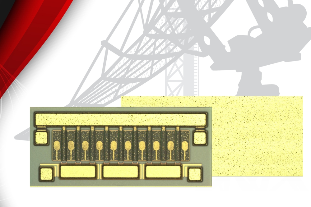
One example of this is a chip that features 800, 1.3 µm emitters (see Figure 6). Operating in quasi-CW mode, this source can deliver more than 8 W of optical power. If higher peak powers are required, the 2D array can be driven with shorter pulses. For pulses in the 200 to 300 µs range, optical peak power can exceed 40 W.
Figure 6. 1.3 μm, 800 emitter InP 2D VCSEL array
Another avenue that we have pursued, for all our key products, is industrial qualification of their reliability. This may involve stress testing up to 50,000 hours.
While we have come a long way, there’s still much more to do. We are now investing in high-volume production capability, to meet the demand for our InP VCSELs in the markets we’ve discussed. Such efforts will run alongside additional research and development, as we target integration of our VCSELs with silicon photonics, as well as increasing the bandwidth and optical power of our sources. We shall also pursue leading-edge packaging of our VCSELs, and the expansion of their wavelength range beyond 2.3 µm. Without doubt, there’s a very exciting future in store for the InP VCSEL.
Vertilas’ portfolio includes long-cavity BCB 10 Gbit/s VCSELs and short-cavity BCB 25-50 Gbit/s VCSELs.
Key technology milestones of Vertilas InP VCSELs
- 2022: 1.3 µm 2D VCSEL array with 800 emitters and 8 W quasi-CW performance
- 2019: Concept of 2 Tbit/s SiP transmitter with 40 VCSELs at 50 Gbit/s
- 2017: 1.3 µm single mode VCSEL with 40 Gbit/s data transmission (NRZ)
- 2014: 1.55 µm VCSEL with 40 Gbit/s optical data transmission
- 2011: Prototype of wide tuneable 1.55 µm VCSEL with 100 nm tuning range
- 2008: 1.3 µm VCSEL for 12.5 Gbit/s optical data transmission
- 2005: 1.55 µm single mode VCSEL with optical power of 1 mW at 80°C
- 1999 - 2001: BTJ VCSELs at 1.3 µm, 1.55 µm and 2.0 µm
Further reading
- J. Fabrega et al. “Experimental Demonstration of a Metro Area Network with Terabit-capable Sliceable Bitrate Variable Transceiver using Direct Modulated VCSELs and Coherent Detection”, J. Opt. Commun. Netw., Jan 2023
- R. Dohle et al. “New Packaging Technology for Disruptive 1- and 2- Dimensional VCSEL Arrays and Their Electro- Optical Performance and Applications”, 2022 IEEE 72nd Electronic Components and technology Conference (ECTC), May/June 2022
- C. Li et al. “Hybrid integration of VCSEL and 3-µm Silicon Waveguide based on a monolithic lens system”, IEEE Trans. Compon. Packag. Manuf. 12 883 (2022)
- M. Svaluto Moreolo et al “Multi-Tb/s photonic transceivers for metro optical network connectivity evolution“, Proc. of SPIE OPTO, Multi-Tb/s photonic transceivers for metro optical network connectivity evolution, 2021 (online)
- P. Gatto et al. “Beyond 25 Gb/s Directly-Modulated Widely Tunable VCSEL for Next Generation Access Network,” 2018 Optical Fiber Communications Conference and Exposition (OFC) Th1E.2.
- M. Verplaetse et al. “DSP-free and real-time transmission of 50Gb/s NRZ over 15km SSMF and 64Gb/s NRZ B2B with a 1.3 µm VCSEL”, OFC 2018, Th4B.7
- T. Aalto et al. “Transceivers for 400G based on hybrid integrated thick SOI and III/V chips”, ECOC 2017
- N. Eiselt et al. “Experimental Demonstration of 84 Gb/s PAM-4 over up to 1.6 km SSMF Using an 20-GHz VCSEL at 1525 nm”, IEEE Journal of Lightwave technology 35 1342 (2017)
- A. Dochhan et al. “56 Gb/s DMT Transmission with VCSELs in 1.5 µm Wavelength Range over up to 12 km for DWDM Intra-Data Center Connects”, ECOC 2016
- M. Ortsiefer et al. “Long-wavelength VCSELs for TDLS applications“, Field Laser Applications in Industry and Research (FLAIR), Garmisch-Partenkirchen, 2009


