

Taking Ga₂O₃ to the next level
Agnitron’s MOCVD reactors are underpinning tremendous advances in the
material quality of Ga2O3, as well as leaps in the performance of
various power devices made from this ultra-wide bandgap semiconductor.
BY
FIKADU ALEMA, AARON FINE AND ANDREI OSINSKY FROM AGNITRON, ARKKA
BHATTACHARYYA AND SRIRAM KRISHNAMOORTHY FROM UCSB, AND CAMERON GORSAK
AND HARI P. NAIR FROM CORNELL UNIVERSITY
On the back of continuous rapid strides, Ga2O3 devices are poised to shape the future of the power semiconductor market. This ultra-wide bandgap material has all the key characteristics necessary to produce better devices and, at the same time, the potential for cost-competitiveness, thanks to the capability to make high-quality melt-grown bulk substrates.
It is now a decade since device and materials research into Ga2O3 began in earnest. Over that time tremendous progress has been made, in terms of both the quality of the epitaxial material and the performance of Ga2O3 diodes and transistors. Recent reports include β-Ga2O3-based devices with a breakdown voltage over 8 kV and critical breakdown fields beyond 5 MV/cm, a regime that exceeds the theoretical limits of SiC and GaN. Such success establishes β-Ga2O3 as the most promising candidate for next-generation solid-state power-switching applications.
Now is the time to build on all this progress and deliver further improvement to the quality of β-Ga2O3 epitaxial films, as progress on this front will open the door to practical power electronic devices that fully exploit the potential of this oxide. That’s the key message at the heart of this feature, which summarises the latest MOCVD process optimisation that has ensured high-quality materials and ultimately high-performance devices. It is clear that when β-Ga2O3 is grown by MOCVD using optimal process conditions, the resulting material is of unrivalled quality.

Figure 1. 2D thickness map of a Ga2O3 thin film grown on a 50 mm
sapphire substrate using the Agnitron Agilis 100 MOCVD reactor. A 2 mm
edge exclusion is applied to the map. Film thickness is very uniform,
with a non-uniformity of only about 2 percent.
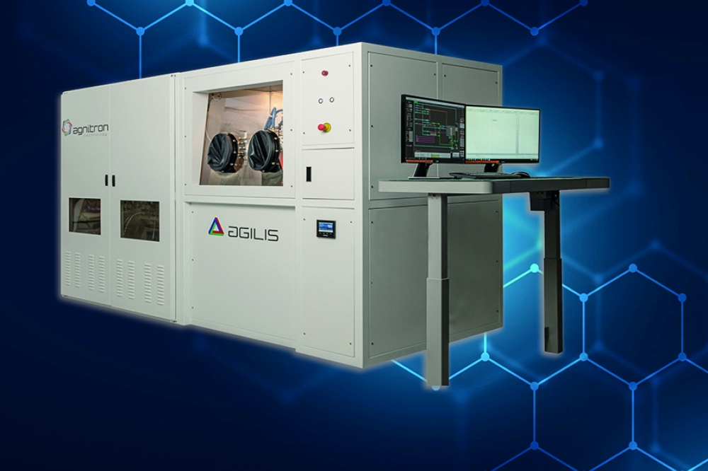
At Agnitron Technology of Chanhassen, MN, we have a well-deserved reputation for being the world’s leading provider of MOCVD reactors for the growth of β-Ga2O3. One of our most well-known tools, the Agilis, is being used in both our laboratory and in various world-class institutions, including: the University of California, Santa Barbara (UCSB); Cornell University; the US Naval Research laboratory (NRL); Iowa State University, the University of Utah, the Ohio State University (OSU), and Bristol University, UK. Researchers from these institutions are greatly satisfied with the top performances of our reactors and continue to produce ground-breaking material and devices results. Here we highlight the results of Ga2O3 grown on our reactors in our laboratory and in the labs of our co-authors at UCSB and Cornell University.
Growing highly uniform films
Thanks to continuous improvements in the supply of large-area Ga2O3 substrates, now available in diameters of up to 100 mm, there’s a compelling need to be able to grow highly uniform thin films, in terms of both thickness and doping uniformity. While our Agilis 100 MOCVD is primarily intended for R&D, using far smaller substrates, it is capable of accommodating wafers up to 50 mm in diameter. Due to this, it is crucial that this reactor can realise uniform films on wafers of such sizes.
Our Agilis 100 employs a unique remote-injection showerhead design. Oxygen enters the reactor from a single central injector with an inert gas push flow, while the gallium metalorganic source, typically tri-ethyl-gallium, is introduced from the showerhead area that surrounds the central oxygen injector, again with an associated push flow. Merits of this design include laminar flow conditions, and prevention of mixing of the oxygen and metalorganic sources until they reach the substrate, thereby mitigating gas phase reactions and an associated reduction in growth rate. Another advantage of separate injection is that it provides an additional knob for fine-tuning the reactor’s gas flow profile.
Following installation of our Agilis 100 MOCVD reactor at Cornell University, we worked together to identify process conditions for increasing the uniformity of Ga2O3 films on 50 mm substrates. We found that through careful tuning of the flows and the reactor pressure, we could produce Ga2O3 films with a thickness non-uniformity of around 2 percent (see Figure 1). To realise the highest uniformity, we combined high total gas flows with low reactor pressures, conditions that are known to mitigate buoyancy associated with flow instabilities [1]. These conditions are conducive to the growth of films with high mobilities and smooth surfaces – measurements have revealed a root-mean-square roughness below 1 nm. The combination of a high carrier mobility and a low surface roughness is essential for the fabrication of high-performance devices over the entire 50 mm substrate.
Another strength of our design of reactor is that thanks to its unique injection system, it is amenable to further modifications. For example, adding a nozzle with a reduced diameter to the central injector increases the velocity of gas flow, and thus ensures a higher growth rate.

Figure 2. Capacitance-voltage measurements determine the doping
concentration dependence of the silane molar flow rate, for the growth
of β-Ga2O3 films at Agnitron Technology using optimal process conditions
(a). 2D atomic force microscopy (AFM) images of 5.1 µm thick layers
grown on (010) β-Ga2O3 substrates with miscut angles of 1º (b) and 0º,
also known as on-axis (c). The features on the film grown on the on-axis
substrate are bigger than those for the film on the substrate with
miscut angle of 1º.
Realising low doping
Due to an absence of p-type doping, most Ga2O3 device architectures are unipolar. This limitation means that there is a need to grow thick epitaxial films with a low doping concentration to realise efficient voltage-blocking power devices. If there is a high doping concentration in the Ga2O3 epitaxial layer, which is also known as the drift layer, the depletion region narrows, resulting in a strong electric field at the junction between the metal and Ga2O3. This high electric field exerts a substantial force on electrons, propelling them across the junction. In turn, the electrical current through the device increases, leading to a threat of electrical breakdown. Due to these concerns, it is far better to have a low doping concentration in the drift layer. When that’s in place, the depletion width increases, reducing the electric field at the junction and thus increasing the breakdown voltage. Note that it’s important that the drift layer is thick enough to either match or exceed the depletion width.
We recommend MOCVD for the growth of devices with a thick drift layer, because this technique offers high-speed growth – a rate of around 10 mm/hr is possible – alongside nanometre surface roughness and uniform doping [2]. Last year, in the pages of this publication, we reported that with this growth technology we had demonstrated free-carrier concentrations that range from around 7 × 1015 cm-3 and around 2.5 × 1016 cm-3, for unintentionally doped and lightly silicon-doped β-Ga2O3 films, respectively. Recent process optimisation has improved these figures, with the realisation of even lower doping concentrations that have a tremendous advantage for vertical power devices. Our latest breakthrough came from film growth at a reduced growth pressure of less than 20 Torr, which drives down gas phase reactions and lowers defects and inclusions in the film.
Capacitance-voltage measurements (see Figure 2 (a)) on our epitaxial films unveiled the relationship between their doping concentration and the molar flow rate for silane (SiH4/N2). This study showed that the doping concentration varied linearly with silane molar flow rate, as expected. However, the key breakthrough is that when we dialed the silane molar flow rate down to around 3 × 10-12 mol/min, the doping concentration in the film fell to around 1.5 × 1015 cm-3.

Figure 3. The channel structure used for uniformly and intentionally silicon-doped films for the doping range of 1017–1020
cm−3, grown using Agnitron’s Agilis 100 (a). Room-temperature Hall
mobility of the channel stacks as a function of Hall carrier density,
benchmarked with various state-of-the-art reports (b). Effectiveness of
the growth steps is confirmed by Cornell University, using the same
Agilis 100 reactor. Details of the data in (b) can be found in reference
[5].
Miscut merits
One of the big challenges with vertical power devices grown using MOCVD is that the growth of the thick, low-doped drift layer can lead to the formation of macro defects, with hillocks, particles, and pits forming on the film’s surface. The drift layer may need to have a thickness of tens of microns, but after around 3 µm of growth its surface is hampered by the defects just described, leading to a high surface roughness of more than 5 nm. Compounding matters, as film thickness increases, the defects get larger and more abundant.
Multiple origins are to blame for the surface defects in these epilayers. They can be traced back to the substrate, the growth process conditions and the substrate preparation methods. For example, researchers from the University of Utah that are using our Agnitron reactor recently observed the propagation of line defects, such as nanopipes, into the epitaxial layers out of the substrates [4]. Left unmanaged, these defects will degrade film quality and account for the premature breakdown of devices.
The issues seen in MOCVD growth are also present in films formed by halide vapor phase epitaxy (HVPE), an alternative approach for growing thick layers of β-Ga2O3. When growing Ga2O3 by HVPE, there’s a need to smooth the extremely rough epitaxial layers with chemical-mechanical polishing. However, this post-growth polishing hampers efforts to realise sharp doping profiles and abrupt heterointerfaces, not to mention the challenge with the lateral doping inhomogeneity to begin with. With MOCVD, it’s possible to minimise surface defects by optimising the growth process and using a suitable substrate with a few degrees miscut.
We have investigated the influence of low-pressure optimal process conditions on the surface quality of thick b-Ga2O3 films. Using the process conditions for a doping concentration of low 1015 cm-3, we grew a 5.1 µm-thick lightly doped β-Ga2O3 epitaxial layers on two (010)-oriented tin-doped substrates. Co-loaded into the reactor, this pair of substrates had different orientations: one was a regular on-axis substrate, and the other had a 1° miscut. Inspecting these films revealed that the surface quality improved with optimal process conditions (see Figures 2 (b) and 2 (c), showing atomic force microcopy images of 20 µm by 20 µm scan areas). The epilayers on both substrates have a smooth surface, but the value for the root-mean-square roughness is lower for that with a miscut foundation, at just 0.59 nm.
One of the key benefits of a low growth pressure is that it minimises the gas phase reaction in the chamber, thereby reducing the formation of particles that can land on the substrate and act as a seed for the nucleation of defects. The upshot is a trimming of the defect density in the epilayers.
Combining this low growth pressure with a substrate with a few degrees of miscut leads to further gains, in terms of the surface quality of the films. Thanks to the introduction of terraced surfaces, in the miscut wafers, there is the potential to enhance diffusion of gallium adatoms on the substrate’s surface during the growth process.
Our initial studies have identified the importance of investigating whether β-Ga2O3 substrates with higher miscut angles can lead to a further reduction in surface defects on thick films. Our plan is to study (010) β-Ga2O3 substrates with miscut angles between 2° and 4°.
Enhancing channel mobility
A very active area of β-Ga2O3 material research is associated with attempts to increase the channel mobility in β-Ga2O3 epitaxial films. A higher channel mobility is a prized asset, essential to realising a low on-resistance that leads to low conduction and switching losses in devices, and ultimately to ensuring minimal energy waste in power circuits.
Working at UCSB, Sriram Krishnamoorthy’s team have been using an Agilis 100 reactor to carefully tune MOCVD processes and enhance the electron mobility of films with a wide range of doping concentrations [5]. These efforts have included the development of a substrate cleaning process involving hydrofluoric acid, and the introduction of a hybrid channel structure with low-temperature buffer layers. The latter led to record-breaking electron mobility for both uniformly silicon-doped (3D doped) and δ-doped (2D doped) Ga2O3 epitaxial films grown on (010) iron-doped bulk substrates. For substrate cleaning, the team started with solvent cleaning, followed by treatment for 30 minutes in HF (49 percent in water) and then in-situ oxygen annealing in the MOCVD reactor prior to epilayer growth. This procedure produced an atomically smooth surface and compensated for any undesired low-mobility electron channel at the interface between the epitaxial layer and the substrate.

Figure 4.The tri-gate β-Ga2O3 MESFETs (with a SiNx wrap-around passivation not shown) feature a high-mobility channel stack with low-temperature buffer layers (a). (b) Benchmark plot of the differential specific on-resistance as a function of blocking voltage for tri-gate β-Ga2O3 MESFETs, with literature reports showing record transistor performance [6].
To produce the channel structure, those at UCSB modulated the epitaxy growth temperature from 600 °C, used for growth of the un-doped Ga2O3 buffer layer and then the transition layers, to 810 °C for the silicon-doped Ga2O3 channel layers (see Figure 3 (a)). Note there was no growth interruption. For doping ranging from 2 × 10¹⁶ to 1 × 1020 cm−3, this structure provided room-temperature Hall mobilities of 196 - 85 cm2 V-1 s-1 – that’s an enhancement in electron mobility of around 30-50 percent over this doping range (see Figure 3 (b)). At Cornell University comparable results for mobility have been reported using similar process conditions, again using the Agilis 100 system (see Figure 3 (b)). Taken together, these very promising results from two world-class universities champion the versatility of our reactor, and highlight its capability to break new ground, in terms of both epitaxy and device development. The team at UCSB have also produced δ-doped channels with sheet charge of 9.1 × 1012 cm−2 that provided a mobility of 110 cm2 V-1 s-1.
Lateral devices
Lateral transistors that utilise these uniformly silicon-doped channels with low-temperature buffers exhibit state-of-the-art performance (see Figure 4(a)). These devices produce a very low reverse leakage for breakdown voltages up to 3 kV. What’s more, thanks to enhanced electron mobility, they exhibit low on-state resistances. Combining these virtues with effective electric-field management leads to a figure of merit for power as high as around 1 GW cm-2, a new record for Ga2O3 transistor device technology (see Figure 4 (b)) [6].
In addition to this progress in lateral transistors, there have been significant, recent advances in lateral diodes based on materials grown using the Agilis 100 reactor. Those at UCSB have fabricated a novel lateral β-Ga2O3 Schottky barrier diode featuring a high permittivity dielectric superjunction structure, leading to a breakdown voltage of −1487 V. The performance of this diode makes it an attractive candidate for low-to-medium voltage applications that require lower conduction losses. Normalizing to the active current-conducting area yielded a power figure-of-merit of 2.7 GW cm-2 – that’s higher than the SiC’s unipolar power figure of merit [7]. While this high value comes from the superjunction effect, with the strength of the electric field inside the lateral drift region reduced through the distribution of the depletion region over the entire length of the diode, it is the MOCVD grown material that makes this possible.
15 Years of MOCVD
The common thread that links all the great results just discussed is that they have been obtained using Agnitron’s MOCVD tools. Agnitron this year will be celebrating 15 years of innovation and cutting-edge technology.
By continuing to develop Agnitron’s systems for MOCVD of β-Ga2O3, Agnitron has enabled them to become more efficient and cost-effective while still providing reliable results. The great versatility of the Agilis 100 explains why it is the most featured and referenced growth tool in this article. Note that its versatility actually makes it a compelling candidate for a wide range of experiments beyond β-Ga2O3.
At the heart of all of Agnitron’s tools is a proprietary vertical growth chamber that features a high-speed rotating disc reactor (RDR), capable of operating at over 1300 revolutions per minute. Agnitron minimises the chances that any deposition within the chamber reaches the wafer surface through material science and design engineering. The high-speed RDR’s unique flow dynamics repress particle recirculation, leaving areas above the wafer clean and free of deposition. Another virtue of the high-speed rotation of Agnitron’s RDR is that it allows a higher degree of control, ensuring superior thickness distribution uniformity.
The Agilis 100 reactor, developed by Agnitron, is equipped with optical reflectometry in the UV and blue range, enabling users to determine film growth rate and thickness in real-time. This hardware is fully integrated into the Imperium analytical control software. To control the purity of Ga2O3 epitaxial films, Agnitron added the capability to expose a UV light directly on the wafer during the growth process. This method enables management of point defects and further reduces any residual carbon that can incorporate into Ga2O3 films during the MOCVD process. The method is proven effective in MOCVD of GaN, as has been extensively explored by researchers at North Carolina State University [8].
Agnitron had previously demonstrated high purity β-Ga2O3 films with a record low-temperature electron mobility of more than 23,000 cm2 V-1 s-1 and acceptor concentration of 2 × 1013 cm-3 using one of its Agilis reactors [9]. This was achieved by mitigating the carbon incorporation into the films through process conditions. But, with the current UV exposure capability, we believe that a far purer material with robust process reproducibility can be achieved.
Agnitron’s MOCVD systems, especially the Agilis 100, are highly flexible, allowing operators to switch between various sources by adding a few hardware components. Moreover, within two hours of maintenance, regardless of the source selected, users can change the gas distribution configuration between remote and close-injection delivery. This option provides researchers with the convenience to experiment and enhance their processes effortlessly. Additionally, extra nozzles can be attached to the gas distribution flanges, which can be used to refine the process or clean the wafer carrier. This range of desirable features makes Agnitron’s reactors an attractive alternative for various applications.
To address the high cost of wafers and gas consumption in R&D, there is a need to grow on a single large-area wafer. Agnitron’s β-Ga2O3 MOCVD reactors, specifically the Agilis 500/700, can now accommodate wafers up to 100 mm and 160 mm in diameter, respectively. These larger multi-wafer reactors maintain the same footprint as the Agilis 100 and were responsible for some of the results in this article. This expansion provides excellent capability for scientists interested in growing larger diameter wafers for a matching fab line.
Agnitron will soon expand its oxide portfolio with the GOX 300, a fully automated production Ga2O3 MOCVD system offering further capabilities for larger wafers. Additionally, the company added the Agilis Mini to its range. This reactor is equipped with the same capabilities as the Agilis 100, but with a smaller footprint and a more cost-effective price.
Agnitron has developed a patent-pending technology that upgrades the close-injection gas distribution system, ensuring oxygen injection across the entire wafer carrier, rather than just centrally. This system, in combination with Agnitron’s RDR fast rotation, leads to superior thickness and doping uniformity of epitaxial layers.
Agnitron’s hardware engineering department continues to make improvements and advancements to its MOCVD tools, ensuring that each new generation of reactor provides greater reliability and versatility for process engineers. These breakthroughs pave the way for future advancements in high-voltage power devices.
Equipment and process development results discussed in this article were partly funded by the Office of Naval Research (ONR) through the STTR Phase II program, contract number N6833518C0192, under the direction of Mr. Lynn Peterson, and Air Force’s AFWERX SBIR Phase I program, Contract Number: FA8649-21-P-0304.

Figure 5. The Agnitron Agilis 100 and Mini MOCVD systems offer maximum flexibility with their ability to feature both remote injection and close injection showerhead flanges, enabling users to quickly and easily switch between the two options to optimise their processes. Furthermore, the close injection showerhead flanges are designed with multiple preset distances from the wafer to increase experiment flexibility. The blue light is for optical reflectometer for in-situ monitoring of the films growth rate.
Agilis 100 reactor with UV light source exposure
Testimonials for Agnitron Technology
Hari P. Nair, Cornell University
“Agnitron’s Agilis 100 MOCVD system was installed in my lab in the summer of 2022. Within a span of two days, we were able to demonstrate all the material’s quality specs needed for the acceptance of the system and achieve high-quality gallium oxide epitaxial films on par with other leading gallium oxide research groups around the country, which by the way, were also grown using Agilis 100 MOCVD systems. This is a testament of the consistent high performance of the Agilis platform. The Agnitron team provides excellent support to their customers. They are very committed to ensuring that their customers get the best out of their systems. They promptly respond to questions that arise, be it related to growth parameters or general troubleshooting.”
Sriram Krishnamoorthy, Materials Department, UCSB
“I started out my research group at The University of Utah and ordered one of the first Agnitron Agilis 100 MOCVD systems, after taking notice of the early research breakthroughs from the in-house gallium oxide epitaxy research at Agnitron. This platform enabled us to make rapid strides in demonstration of impressive material quality and the associated device performance, within such a short time frame. When my research group moved to UCSB, it became an obvious choice to double down on the Agilis 100 system and we are currently installing it. I’m beyond excited to see where this takes us. I have ordered a brand new MOCVD system from Agnitron with two different showerhead geometries to capitalise on the enormous possibilities enabled by the Agnitron MOCVD platform and the system will be installed soon in UCSB’s Institute of Energy Efficiency (IEE) building, Henley Hall.”
Michael A Scarpulla, University of Utah
“Agnitron has been a remarkable equipment supplier and material and process development partner for the University of Utah. From the planning phase for acquiring our Agilis reactor to more recent collaboration on growing layers designed for specific studies of point defects, Agnitron’s staff have always been in open communication and working together to get the best performance. I’m impressed that they not only supply good machines, but have also been setting records in terms of material quality too. They have also worked through equipment challenges and collaborated with us on developing the procedures for optimal epitaxial growth. Agnitron is a superb equipment supplier but also R&D partner – this is a rarity in my more than 20 year research career.”
Houqiang Fu, Arizona State University
“Agnitron is a top supplier of MOCVD reactors for various materials systems. They capitalise on their R&D laboratory to demonstrate record-performance materials on similar tools that they sell. While at Iowa State University, I bought an Agnitron Agilis 100 oxide reactor; I’ve now moved to ASU, and it was an easy decision to utilize Agnitron again. In fact, my ASU colleague (Dr. Nidhin Kurian Kalarickal) and I have purchased two Agnitron Agilis tools. An Agilis-100 for oxides and an Agilis-mini for high-temperature nitrides. Agnitron has been great to work with from start to finish. They support everything from pre-delivery facility preparation to troubleshooting issues after delivery. Their staff are patient and responsive, always helping us solve problems and optimise growth recipes. One of their strengths is the willingness to customise reactors for unique research needs.”
Further reading
[1] C. R. Biber et al. J. Cryst. Growth 123 545 (1992)
[2] F. Alema et al. J. Cryst. Growth 475 77 (2017)
[3] F. Alema et al. CS Magazine 28 (2) 16 (2022)
[4] J. Cooke et al. J. Vac. Sci.Technol. A 41 013406 (2023)
[5] A. Bhattacharyya et al. APL Mater. 11 021110 (2023)
[6] A. Bhattacharyya et al. IEEE Electron Dev. Lett. 43 1637 (2022)
[7] S. Roy et al. IEEE Electron Device Lett. 43 2037 (2022)
[8] S. Rathkanthiwar et al. Appl. Phys. Express 15 051003 (2022)
[9] G. Seryogin et al. Appl. Phys. Lett. 117 262101 (2020)


