Loading...
News Article

ST to build world’s first fully integrated SiC facility in Italy

News

High-volume 200mm SiC facility for power devices, modules, test and packaging, to be built in Catania, Italy

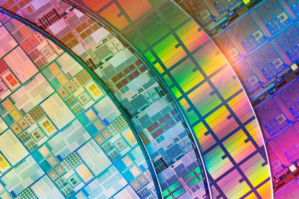
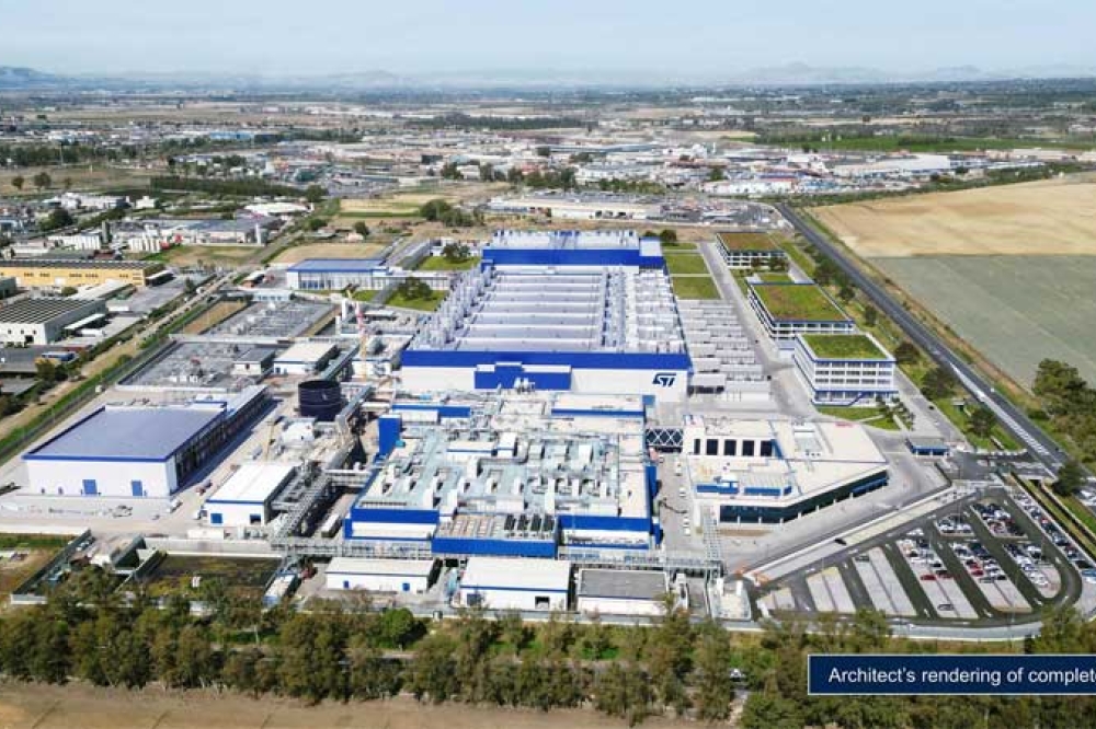
STMicroelectronics has announced a new high-volume 200mm SiC anufacturing facility for power devices and modules, as well as test and packaging, to be built in Catania, Italy.

The total investment is expected to be around €5B, with support of around €2B provided by the State of Italy within the framework of the EU Chips Act.

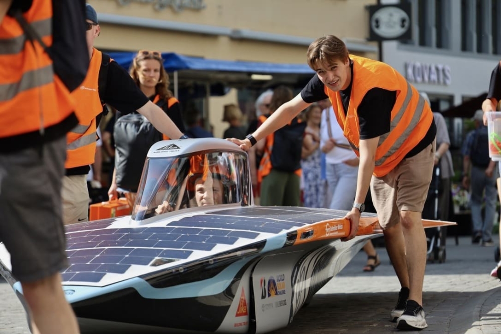
Combined with the SiC substrate manufacturing facility being readied on the same site, these facilities will form ST’s SiC Campus, realizing the Company’s vision of a fully vertically integrated manufacturing facility for the mass production of SiC on one site. ST says the creation of the new SiC Campus is a key milestone to support customers for SiC devices across automotive, industrial and cloud infrastructure applications, as they transition to electrification and seek higher efficiency.

“The fully integrated capabilities unlocked by the SiC Campus in Catania will contribute significantly to ST’s SiC technology leadership for automotive and industrial customers through the next decades,” said Jean-Marc Chery, president and CEO of STMicroelectronics. “The scale and synergies offered by this project will enable us to better innovate with high-volume manufacturing capacity, to the benefit of our European and global customers as they transition to electrification and seek more energy efficient solutions to meet their decarbonization goals.”

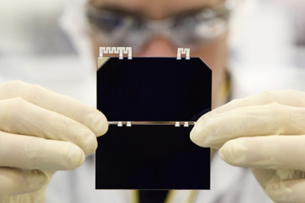
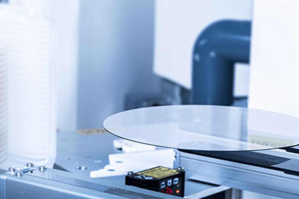
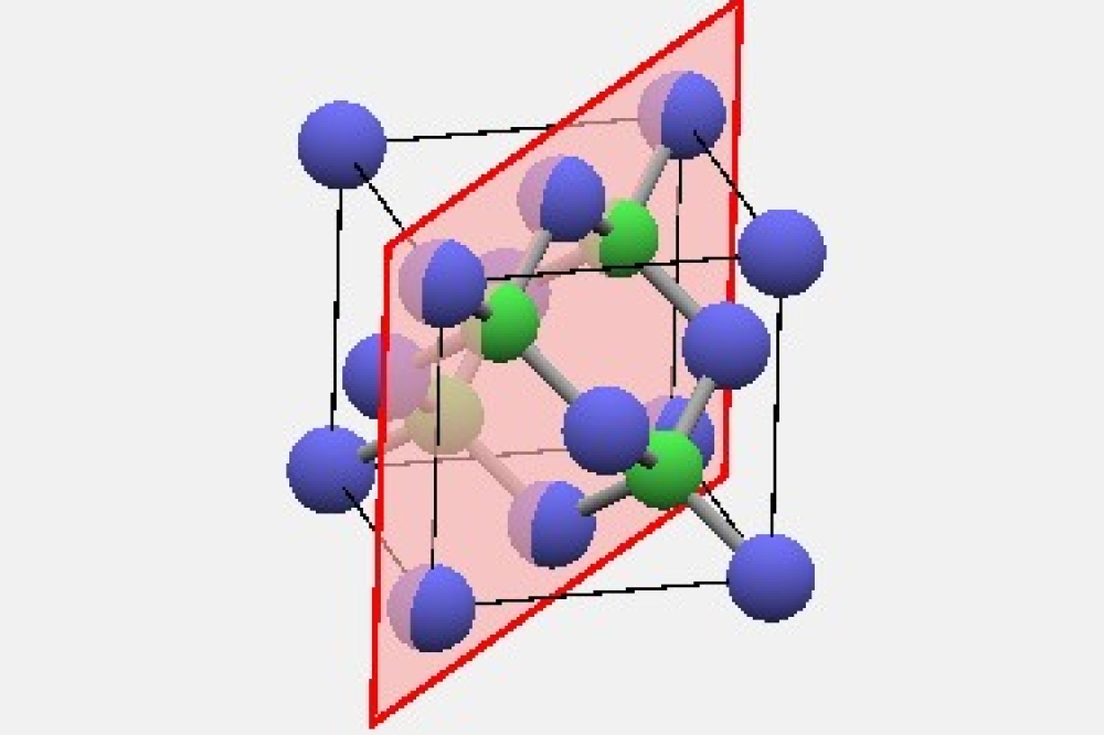
The SiC Campus will serve as the center of ST’s global SiC ecosystem, integrating all steps in the production flow, including SiC substrate development, epitaxial growth processes, 200mm front-end wafer fabrication and module back-end assembly, as well as process R&D, product design, advanced R&D labs for dies, power systems and modules, and full packaging capabilities. This will achieve a first of a kind in Europe for the mass production of 200mm SiC wafers with each step of the process – substrate, epitaxy & front-end, and back-end – using 200 mm technologies for enhanced yields and performances.

The new facility is targeted to start production in 2026 and to ramp to full capacity by 2033, with up to 15,000 wafers per week at full build-out. Sustainable practices are integral to the design, development, and operation of the SiC Campus to ensure the responsible consumption of resources including water and power.

SPONSOR MESSAGE

Secure Your Hydrogen Supply

A study supply of high-purity hydrogen is critical to semiconductor fabrication. Supply chain interruptions are challenging manufacturers, leading to production slowdowns and stoppages. On-site hydrogen generation offers a scalable alternative for new and existing fabs, freeing the operator from dependence on delivered gas.

Plant managers understand the critical role that hydrogen plays in semiconductor fabrication. That important job includes crystal growth, carrier gas, wafer annealing, and in the emerging Extreme UV Lithography (EUV) that will enable new generations of devices. As the vast need for semiconductors grows across all sectors of world economies, so does the need for high-purity hydrogen.

Take control with Nel on-site hydrogen generation.

Read more
Ascent wins order for power beaming Space PV module
Navitas Partners with Great Wall for 400V-DC power
SemiQ supplies SiC MOSFET modules for EV battery cell cyclers
Coherent and Keysight collaborate on 200G/lane multimode VCSEL tech
Lumentum and Marvell exhibit integrated 450G optical interface
Marktech announces new MWIR LEDS
Imec identifies stable range for GaN MISHEMTs in RF PAs
Polar Light completes $3.4m funding round
Lynred launches advanced thermal imaging modules
Altum RF expands Sydney design centre
Sivers announces partnership with O-Net
Ayar Labs unveils first UCIe optical chiplet
Aixtron delivers InP tool to Nokia
WHU-USTC team demo novel temperature monitoring of GaN device
Phlux lands £9m to take InGaAs sensors to next level
4-inch gallium oxide facility established in Swansea
Mazda and Rohm collaborate on automotive GaN
University of South Carolina chooses MOCVD tool from TNSC
Wolfspeed appoints new CEO amidst funding crisis
SiC slowdown is only short term, says Yole
Pragmatic launches flexible IGZO-based NFC chip
Poet ships latest optical engine samples
EU project to develop 1200V DC powertrain
£250m to turbocharge Welsh compound semi cluster
Scientists harness phonon-polariton electroluminescence
TU Graz team reveals the secrets of heat conduction
Aixtron to partner in ‘GraFunkL‘ UVC project
EU collaboration steps up heterogeneous design
Diodes Inc announces InSb sensors
Far-UVC module targets close-quarters disinfection
Sivers and WIN collaborate on DFB laser production
Boosting the blocking voltage of birectional HEMTs
×
Search the news archive

To close this popup you can press escape or click the close icon.
Logo
x
Logo
×
Register - Step 1

You may choose to subscribe to the Compound Semiconductor Magazine, the Compound Semiconductor Newsletter, or both. You may also request additional information if required, before submitting your application.


Please subscribe me to:


You chose the industry type of "Other"

Please enter the industry that you work in:
 
x
Adblocker Detected
Please consider unblocking adverts on this website