Cost-effective SiC
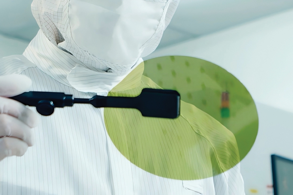
Novel 150 mm SiC engineered substrates, produced using dummy-grade material reuse, unlock the door to cost-effective manufacture of 1200 V SiC MOSFETs.
BY XINHUA WANG AND XINYU LIU FROM INSTITUTE OF MICROELECTRONICS OF THE CHINESE ACADEMY OF SCIENCE, YUHAO ZHANG FROM VIRGINIA TECH, AND FENWEN MU FROM TJ INNOVATIVE SEMICONDUCTOR SUBSTRATE TECHNOLOGY COMPANY
Within the SiC industry, there’s an urgent need for expanded production capacity of SiC substrates, to support the growth of this sector. Hampering efforts to fulfil this demand is the low yield of nearly defect-free substrates suitable for MOSFET manufacture – yield for ‘prime-grade’ material is typically just 40-60 percent. Falling short and leading to significant manufacturing inefficiencies are the inferior low-grade ‘dummy’ substrates, which are naturally produced during the growth and refining of 6-8 inch SiC and often disposed of. Due to these inefficiencies, alongside the complexity, high-energy requirements and challenges associated with the growth of bulk SiC, these substrates have a number of weaknesses. They are renowned for their high carbon footprint and high production cost, often accounting for more than 50 percent of the cost of the MOSFET.
To address this bottleneck, our partnership between the Institute of Microelectronics at the Chinese Academy of Science, Virginia Tech, and TJ Innovative Semiconductor Substrate Technology Company has introduced a novel 150 mm single-crystal SiC-SiC composite substrate, realised with surface-active bonding (SAB) technology. By turning to this engineered substrate, it’s possible to re-use dummy-grade
Figure 1. The main steps in the fabrication process for 6-inch SiC-SiC bonding. The prime-grade SiC substrate is selected for MOSFET fabrication. The dummy-grade SiC substrate is usually adopted in low-grade SiC diode fabrication or treated as waste. The re-use of prime grade SiC allows a reduction in wafer cost. Soft Ar+ bombardment and intentional soft doping activated the SiC surface. After bonding, high-temperate annealing induced a splitting of the prime-grade SiC. Then, ultra-high temperature annealing repaired damage generated during the H+ implantation and interface bonding. A high bonding and transfer rate of 100 percent was achieved, excluding the 1 mm region from the wafer edge. Note that it is very challenging for chemical-mechanical polishing technology to control the uniformity for a high-quality surface layer with several hundred nanometres.
One of the key merits of this approach is that our engineered substrate is capable of potentially cutting costs by 40 percent, compared with prime substrates. In addition, our technology is more sustainable than other approaches, thanks to waste material reuse that avoids the need for new materials. Note that there is no use of poly-SiC substrates with our methodology.
To illustrate the performance and the strengths of our new engineered-substrate technology, we have undertaken a holistic set of experiments, from substrate bonding and epitaxial growth to device fabrication and circuit testing. We have carried out this work using an industrially relevant scale, involving device fabrication from 150 mm wafers at wafer scale, and extensive 150 mm wafer mapping, to characterise both material and devices.
Highlights that have emerged from this effort – and read on to discover all the crucial details – include engineered substrates with a low defect density and a low thermal boundary resistance, and the fabrication of robust, reliable devices with a very high yield. This impressive collection of results underscores the great potential of our new substrate technology for opening the door to more economical and sustainable SiC power electronics.
Figure 2. Benchmarking of the thickness deviation of the transferred semiconductor film as a function of wafer size.
Superior substrates
In general, the current approach that’s adopted within the SiC industry is to reserve prime-grade SiC substrates for high-performance MOSFETs, and to use dummy-grade SiC substrates –characterised by lower crystalline quality and a higher defect density – for low-cost diode production, or to discard as waste.
We are not alone in using engineered substrates to address this weakness in material efficiency. However, while we use surface-activation bonding to integrate a thin layer of prime-grade SiC onto a dummy-grade SiC substrate, the approach taken by Soitec and Sumitomo differs, involving the bonding of a prime-grade SiC thin layer onto a polycrystalline SiC substrate.
To fabricate our SiC-SiC composite substrates, we begin by bombarding prime-grade wafers with H+ ions, with implantation at 90 keV using a fluence of 6 x 1016 cm-2. After this initial step, which forms a pre-fractionation layer, we bond prime- and dummy-grade substrates at room temperature under high vacuum, after activating the surface with an energy ion beam and intentional doping. Subsequent annealing at more than 870 °C splits the pre-fractionation layer, allowing transfer of a prime-grade SiC film around 410 nm-thick to a dummy-grade handle wafer. Finally, annealing at more than 1700 °C repairs the bonding interface, before we apply a handful of finishing steps to improve the roughness and thermal stability of the epi-ready surface (all these steps for fabricating our SiC-SiC composite substrates are illustrated in Figure 1).
We are not alone in forming engineered wafers via the application of a high-quality film on one material to a thicker, lower-quality foundation. To assess our results, we have benchmarked our composite wafer against others with a 150 mm diameter, an exercise that reveals a record low thickness deviation for our material (see Figure 2).
Another encouraging result is that, according to defect mapping, while the number of defects – including pits, micropipes, and bar-shaped stacking faults – totals 206 in a typical dummy-grade substrate, it’s just 59 in our engineered substrate.
Figure 3. Cross-sectional high-resolution transmission electron
microscopy images of the SiC-SiC bonding interface (a) before and (b)
after annealing. The amorphous layer generated during bonding is well
recrystallised by ultra-high-temperature annealing, with only a slight
twist due to the wafer alignment in plane.
Evaluating the boundaries
According to transmission electron microscopy images of the bonding interface before and after annealing (see Figure 3), this step recrystallises the amorphous SiC layer that’s 2-3 nm thick, and formed in the prior step of surface activation. Thanks to this, interface quality improves.
We have turned to electrostatic force microscopy to characterise the electric-field distribution and potential barrier at the bonding interface – both play critical roles in high-current conduction.
The principle of electrostatic force microscopy is a scanning process to measure the cross-sectional potential variation, with the signal amplified by tuning DC and AC biases (see Figure 4 (a)).
With this technique we have determined that annealing produces a reduction in the peak electric field at the bonding interface, which falls from 20.2 kV cm-1 to 8.1 kV cm-1 (see Figure 4 (b) and (c)). Reducing the peak electric field ensures a smaller barrier for carrier flow across the bonding interface. Further evidence for annealing producing a smaller barrier to carrier transport across the bonding interface comes from an ohmic current-voltage test structure, which maintains linear current-voltage characteristics, even at temperatures up to 175 °C. This confirms the robust ohmic contact through the bonded interface.
To determine the thermal boundary resistance of our bonding interface, we have employed transient thermo-reflectance (see Figure 5 (a)). We have a high degree of confidence in this measurement, based on good fitting (see Figure 5 (b)), the Monte-Carlo analysis histogram (see Figure 5 (c)), and sensitivity analysis (see Figure 5 (d)). We have measured a thermal boundary resistance at the SiC-SiC bonding interface of 2.8 +1.4/-0.7 m2 K GW-1 at 25 °C. Benchmarking indicates that our thermal boundary resistance is amongst the lowest values reported for the SiC interfaces bonded with SiC, GaN, and Ga2O3.
Figure 4. (a) An illustration of electrostatic force microscopy
(EFM) scanning at the SiC-film/SiC-sub bonding cross-sectional
interface. The derived electric-field profile images (b) before and (c)
after annealing, respectively, as well as cross-sectional topography and
corresponding apparent surface-potential images in the inset. Set VDC of 5V, VAC
of 0.5V for EFM scanning. Note the potential data shown in the inset
are after signal amplification. The derived potential barrier is below
130 mV, allowing easy tunnelling by electrons in the n++ SiC.
Demonstrating devices
We have used our 150 mm engineered substrates to produce industrial-standard 1.2 kV SiC devices. Following epitaxy, we employed a Candela metrology tool to map our 2 mm x 2 mm die and identify killer defects, including downfalls, micropipes, triangular and carrot defects. Based on this mapping, our killer-defect-free epi yield is very high – it’s 99.2 percent (see Figure 6).
From this epiwafer we have fabricated 1.2kV planar-gate SiC MOSFETs with an on-resistance of 20mΩ. To evaluate these devices, we have considered the key signatures of extrinsic reliability: the gate leakage current (IGSS) and the drain leakage current (IDSS). Mapping for both characteristics, using a gate-source voltage of -4 V for IGSS and a drain-source voltage of 1200 V for IDSS, has allowed us to probe 550 devices across our entire 150 mm wafer. Applying the very stringent standard of an IGSS of below 20 nA and an IDSS of less than 2 mA, determined yields for IGSS and IDSS of 90 percent and 70 percent, respectively (see Figures 7). Such high device yields validate the high quality of our SiC epilayers on our engineered substrates.
We have also recorded the output current-voltage characteristics of our MOSFETs up to 100 A, at 25 °C and 125 °C. From these plots we extracted a specific on-resistance of 3.5 mΩ cm2, which contains a contribution of about 15 percent from the engineered substrate – it has a resistivity of 0.25 W Ωm, and a thickness of 200 µm. At 125°C, there is an increase in on-resistance by around just 20 percent, from a low IDS up to 150 A. This small increase is superior to some reference products on the market.
Figure 5. (a) Schematic of a transient thermo-reflectance (TTR)
measurement of bonded SiC-on-SiC. Pump beam is a 3 ns, 355 nm pulsed
laser and the probe beam is chosen with a 785 nm continuous-wavelength
laser. (b) TTR signals for bonding interface and the best-fitted curve
from the analytical model. (c) Monte-Carlo analysis histogram of thermal
boundary resistance (TBR), measured at room temperature. (d)
Sensitivity of the TTR signal to the TBR signals of SiC-SiC and SiC-Al
interfaces and the SiC thermal conductivity (k4H-SiC). The
sensitivities to three free variables do not significantly overlap in
the time windows and are suitable for simultaneous fitting. Here the
aluminium electrode acts as the metal transducer.
These results validate the stability of our engineered substrate under high IDS at high temperatures. We are also encouraged by the off-state characteristics of our devices at up to 175 °C under 1 mA test compliance. These measurements reveal an IDSS of around 10-8 A up to 800 V at 175 °C. This validates the low epiwafer defect density.
We have also undertaken a hard turn-on and turn-off assessment of our devices, using a 800 V/50 A double-pulse test. The zoom-in waveform allows us to extract rise and fall times of 18.79 ns and 16.97 ns, respectively. These values are comparable to, or even superior to, those for similarly-rated commercial products fabricated on prime-grade substrates reported under a similar double-pulse test condition.
Figure 6. 2 mm x 2 mm die map with an estimated 99.2 percent die
yield of a 6-inch wafer after epitaxial growth. Morphological defects
include downfalls, micropipes, triangular defects and carrot defects.
Reliability and robustness
To evaluate the reliability of the epilayers and the devices that we have produced on our engineered substrate, we have performed high-temperature reverse-bias tests on multiple devices, using a VDS of 960 V and a temperature of 175 °C for 168 hours. This investigation considered four critical device metrics: on-resistance, threshold voltage, blocking voltage and IGSS, both before and after the 168-hour stress. This stress resulted in very small shifts in the four critical metrics: on-resistance, threshold voltage, and blocking voltage changed by less than 1.3 percent; and IGSS shifted by less than 10 percent.
While the bonded substrate does not ‘see’ the high electric field, it does have to pass current between the source and drain. Due to this requirement, its surge-current robustness is critical. To evaluate this, we have used a circuit setup (see (Figure 8 (a)-(c)) that produces a 10 ms-wide half-sine surge current, according to the JEDEC standard. This surge current is generated by an inductance-capacitance resonance, with the peak current controlled by the bus voltage.
Figure 7. (a) IGSS mapping of devices fabricated on 6-inch wafer at VGS of -4 V. Yield is 90 percent. IGSS less than 20 nA (green, pass), between 20 nA and 1 µA (red, failed), more than 1 µA (grey, failed). (b) IDSS mapping of devices fabricated on 6-inch wafer at a VDS of 1200 V. Yield is 70 percent. IDSS less than 2 µA (green, pass), between 2 µA and 99 µA (red, failed), more than 99 µA (grey, failed).
We have recorded the current and voltage waveforms of our devices under surge-current levels ranging from 90 A to 257 A (see Figure 8 (d)). After each test, we comprehensively characterised the SiC MOSFET. We found that this device survived the 245 A surge current test with no degradation, before failing the 257 A test. When inspecting the pin-to-pin resistance of the failed device, we uncovered a gate-source short failure. Investigating this revealed that the ohmic current-voltage behaviour is retained between the drain-source and the drain-gate, suggesting no failure at the bonding interface. If failure occurred here, this would give rise to a potential barrier at the bonding interface, jeopardising the device’s ohmic behaviour.
Figure 8. (a) Circuit schematic, (d) ideal waveforms and (c) photograph of surge current test setup. S1 is first turned on to charge CDC (10 mF), followed by S2 turn-on to produce a inductor-capacitor resonance (L of 1 mH) to generate a 10 ms-width half-sine current waveform for the device under test (DUT). Two 1200V/16mΩ SiC MOSFETs (C3M0016120D) (i.e., S1 and S2) and ten paralleled 1200 V/10 A SBD (C4D10120D) are applied to guarantee higher surge current capability than the DUT. (d) DUT’s current and voltage waveforms under various surge current levels. (e) Pin-to-pin resistances of the failed DUT.
To conclude, our work has showcased the prowess of our novel 150 mm single-crystal SiC engineered substrate produced by surface-active bonding that enables dummy-grade material reuse and prime-grade material recycling. The bonding interface shows the lowest thermal boundary resistance for all SiC bonding reports, and the epiwafers grown on this substrate have achieved a high killer-defect-free yield of 99.2 percent. Additional highlights include 1.2 kV SiC MOSFETs that combine a high yield with good performance and reliability, and surge-current robustness for both device and substrate.
Due to all these encouraging results, we have no doubt that our technology can address the key challenge currently facing the SiC wafer industry, and enable more economical, sustainable SiC power electronics.

