MIT team develops novel low voltage transistor
Silicon transistors are held back by a physical limit (the 'Boltzmann tyranny') that prevents transistors from operating below a certain voltage. But now, in an effort to overcome this limit, MIT researchers have made a novel 3D transistor from ultra thin compound semiconductors.
The resulting device delivers performance comparable to silicon while operating efficiently at much lower voltages than conventional devices. The research was part-funded by Intel and reported in Nature Electronics.
The team's scaled vertical-nanowire heterojunction tunnelling transistors are based on the broken-band GaSb/InAs system. The devices offer a drive current of 300 µA µm−1 and a sub-60 mV dec−1 switching slope at an operating voltage of 0.3 V.
“This is a technology with the potential to replace silicon, so you could use it with all the functions that silicon currently has, but with much better energy efficiency,” says Yanjie Shao, an MIT postdoc and lead author of a paper on the new transistors.
The approach relies on extreme quantum confinement at the tunnelling junction and is based on an interface-pinned energy band alignment at the tunnelling heterojunction under strong quantisation. Quantum confinement occurs when an electron is confined to a space that is so small that it can’t move around. When this happens, the effective mass of the electron and the properties of the material change, enabling stronger tunnelling of the electron through a barrier.
Using tools at MIT.nano, MIT’s facility for nanoscale research, the engineers were able to carefully control the 3D geometry of their transistors, creating vertical nanowire heterostructures with a diameter of only 6 nm They believe these are the smallest 3D transistors reported to date.
Such precise engineering enabled them to achieve a sharp switching slope and high current simultaneously. Because the transistors are so small, the researchers can engineer a very strong quantum confinement effect while also fabricating an extremely thin barrier.
“We have a lot of flexibility to design these material heterostructures so we can achieve a very thin tunnelling barrier, which enables us to get very high current,” Shao says.
Precisely fabricating devices that were small enough to accomplish this was a major challenge.
“We are really into single-nanometer dimensions with this work. Very few groups in the world can make good transistors in that range. Yanjie is extraordinarily capable to craft such well-functioning transistors that are so extremely small,” says senior author Jesús del Alamo, the Donner Professor of Engineering in the MIT Department of Electrical Engineering and Computer Science (EECS).
When the researchers tested their devices, the sharpness of the switching slope was below the fundamental limit that can be achieved with conventional silicon transistors. Their devices also performed about 20 times better than similar tunneling transistors.
“This is the first time we have been able to achieve such sharp switching steepness with this design,” Shao adds.
The researchers are now striving to enhance their fabrication methods to make transistors more uniform across an entire chip. With such small devices, even a 1-nanometer variance can change the behavior of the electrons and affect device operation. They are also exploring vertical fin-shaped structures, in addition to vertical nanowire transistors, which could potentially improve the uniformity of devices on a chip.
“This work definitively steps in the right direction, significantly improving the broken-gap tunnel field effect transistor (TFET) performance. It demonstrates steep-slope together with a record drive-current. It highlights the importance of small dimensions, extreme confinement, and low-defectivity materials and interfaces in the fabricated broken-gap TFET. These features have been realised through a well-mastered and nanometer-size-controlled process,” says Aryan Afzalian, a principal member of the technical staff at the nanoelectronics research organisation Imec, who was not involved with this work.
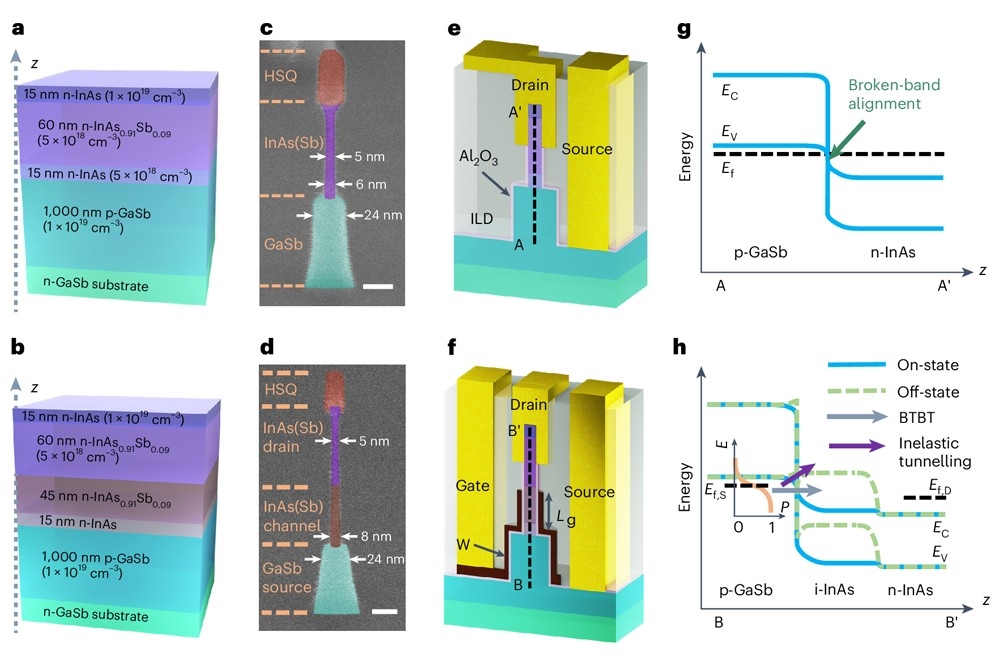
Pictured above: a,b, Heterostructures in the fabrication of a heterojunction Esaki diode (a) and a tunnelling transistor (b). c,d, False-coloured 30°-tilted SEM images of vertical nanowires in the Esaki diode (c) and the tunnelling transistor (d). e,f, Schematics of the finished device structures. g,h, Schematic energy band diagrams for a vertical-nanowire diode and a vertical-nanowire transistor.


