X-FAB and SMART Photonics partner on micro-printing

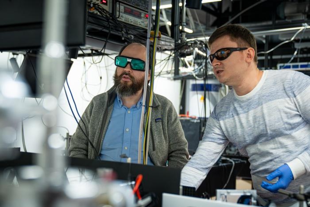
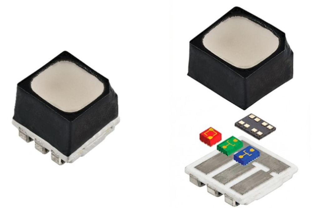
Specialist foundry X-FAB, and InP photonics foundry SMART Photonics have announced a collaboration to integrate X-FAB’s silicon photonics platform with SMART Photonics’ InP chiplets.
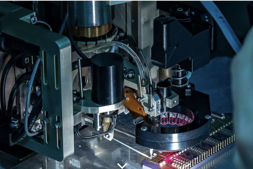
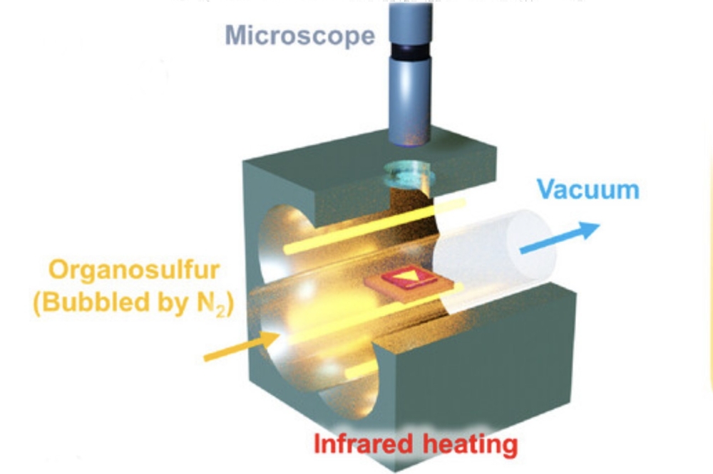
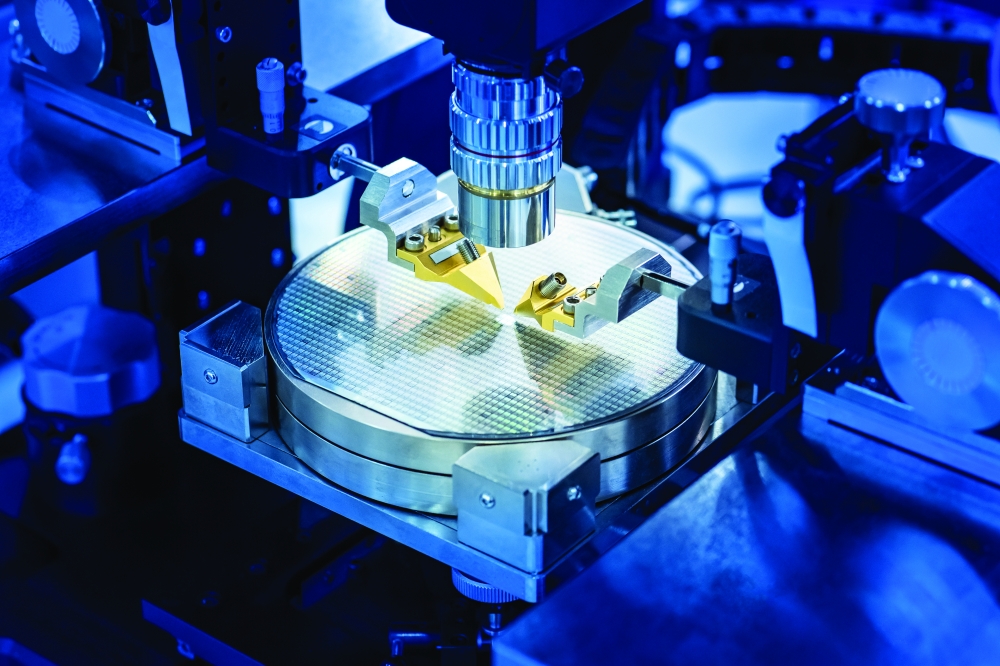
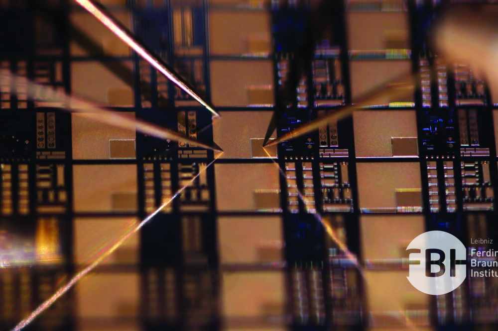
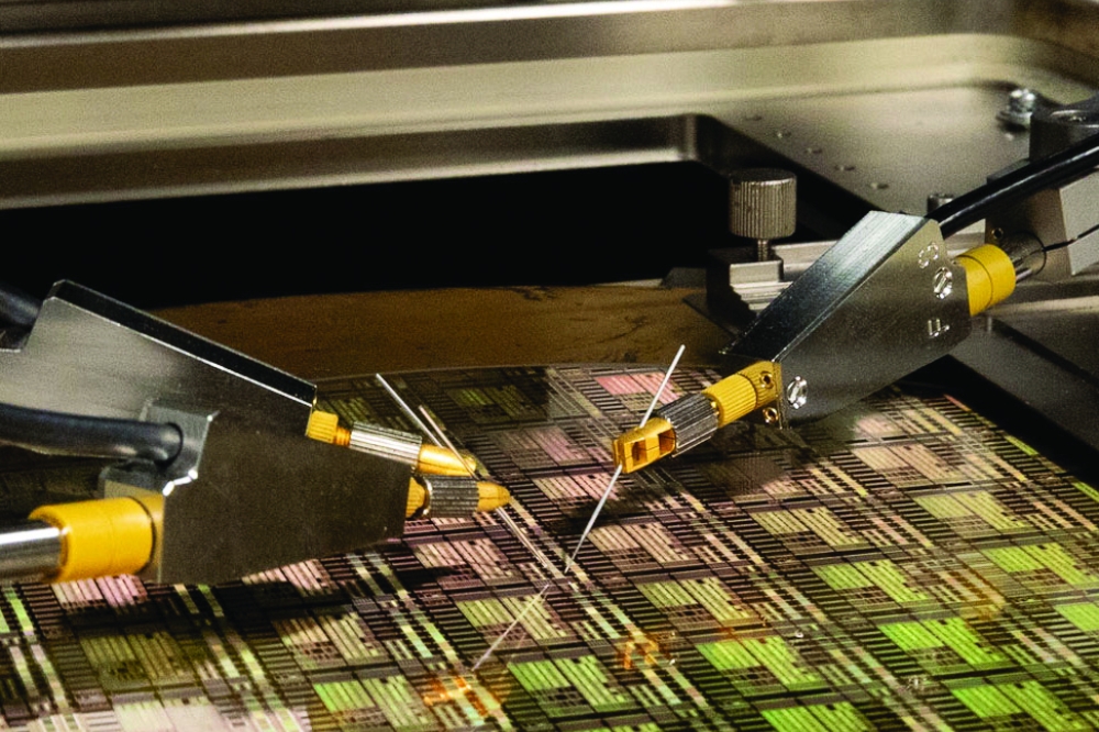
They aim to use use micro-transfer printing (MTP), licensed from X-Celeprint, for heterogeneous integration, enabling new capabilities for datacom and telecom applications.
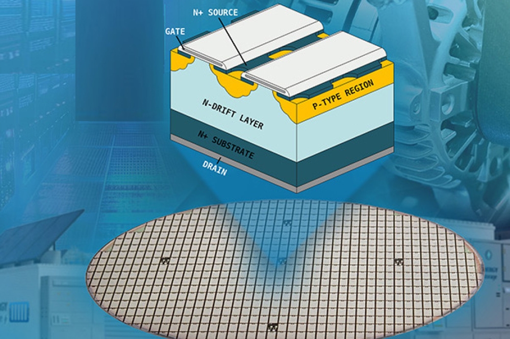
InP technology supports modulator bandwidths exceeding 120 GHz, making it a good solution for next-generation multi-terabit telecom and datacom standards – pushing transceiver speeds far into the terabit realm. In contrast, silicon photonics technologies hit a performance ceiling at around 70 GHz. The collaboration aims to deliver scalable, high-volume solutions that combine the best of both technologies.
By co-optimising silicon photonics, InP, and MTP technologies to fulfill customer requirements, the collaboration will enable new functionalities and improved system performance while reducing integration costs through relaxed photonics packaging requirements.
The MTP technology enables a broad degree of freedom for the system and product designers, by providing flexible integration of various material system chiplets into the product design.
Johan Feenstra, CEO of SMART Photonics, explains: “As the demand for integrated photonics rapidly increases, thanks to the growth of AI and data transfer, our joint solutions will enable much faster data rates while reducing overall power consumption, and therefore the environmental footprint.”
Rudi De Winter, CEO of X-FAB, adds: “Through heterogeneous integration, we are combining the best of the InP and silicon photonics worlds. This will allow our customers to develop innovative solutions addressing the societal challenges of our times such as decarbonization. It is also a great opportunity to build a strong European value chain.”
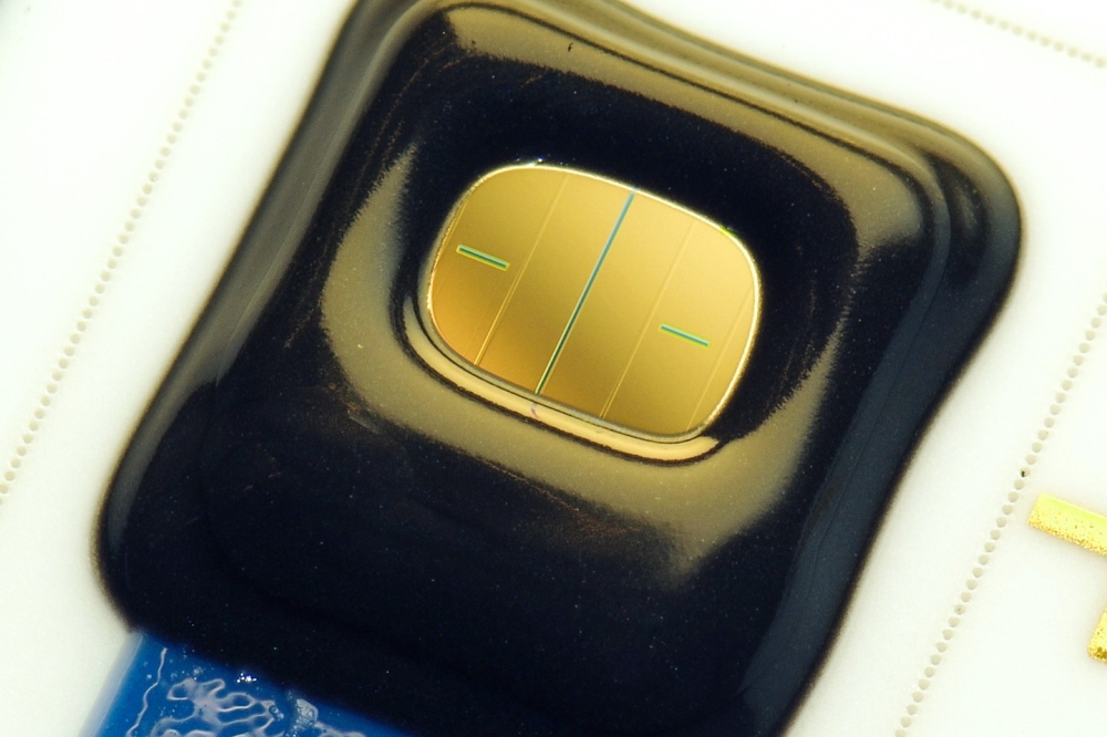
This collaboration builds upon the PhotonixFAB EU funding project, which aims to provide a path to scalable high-volume manufacturing for SOI and SiN silicon photonics, MTP-ready InP chiplets and micro-transfer printing of chiplets.
X-FAB and SMART Photonics recently signed a Memorandum of Understanding to formalise their collaboration. The aim is to support lead customers with industrial prototyping by 2026, with risk production readiness by 2027. Early customer engagements can be supported within the ongoing PhotonixFAB project framework.