

A new approach for 10 kV GaN
A simple plasma-based edge termination approach yields 10 kV-class GaN diodes with a lateral geometry.
BY DAWEI WANG AND HOUQIANG FU FROM ARIZONA STATE UNIVERSITY
Among the competing semiconductor technologies for power electronics, GaN already enjoys significant success. This material delivers an unrivalled performance when there’s a need to block several hundred volts and provide very low power losses. Thanks to these attributes, GaN power devices have established a ‘killer’ application in fast chargers for a range of mobile devices.
Where GaN is yet to make a commercial impact is at voltage ratings of 1.7 kV and more, which are critical for applications like the electric grid, wind turbines, electric drives, and high-voltage power supplies. At these high blocking voltages, the commercial products that are available include silicon insulated-gate bipolar transistors (IGBTs) and thyristors (up to 6.5 kV), and SiC MOSFETs and junction barrier Schottky (JBS) diodes (up to 10 kV). In the labs, researchers have even demonstrated SiC transistors and diodes withstanding up to 30 kV.
However, silicon and SiC devices have significant drawbacks. Due to a bipolar nature, with both majority and minority carriers, high-voltage silicon IGBTs and thyristors are only capable of low switching frequencies and suffer from high switching loss. That’s not an issue for unipolar SiC MOSFETs and JBS diodes, which offer similar high-voltage ratings, and can operate at much higher switching frequencies, thanks to majority-carrier operation. However, commercial SiC high-voltage devices are produced on expensive SiC substrates and need thick epitaxial layers, requirements that lead to an elevated cost per die, due to increased chip size and low yield at high voltages.

Figure 1. Commercial high-voltage vertical silicon and SiC power devices (top) and lateral GaN power devices (bottom).
A potential solution is to increase the operating voltage of GaN power devices, as they have many strengths, including the capability to combine higher efficiencies and temperatures with a reduced footprint, minimal cooling requirements and robust operation. When compared with silicon devices, their far wider bandgap enables either higher voltage ratings with the same thickness, or a similar voltage rating with far less material. Another attribute is the creation of a two-dimensional electron gas with a high mobility, key to allowing GaN power devices to switch far faster than those based on both silicon and SiC. What’s more, GaN power devices can leverage the existing fabrication infrastructure from the mature GaN LED industry for performance improvement, cost reduction, and manufacturability.
At Ariona State University we are working to unleash the capabilities of GaN at high blocking voltages with a simple, damage-free process for producing devices with a lateral geometry.
High-voltage GaN
Uniting commercial high-voltage silicon and SiC power devices is their vertical device geometry. Benefits of this architecture include a high current and a high-voltage capability, a small chip size, immunity to surface issues and good thermal performance.
In contrast, commercial GaN power devices are predominantly lateral high-electron-mobility transistors (HEMTs). This design, used for voltages up to 900 V, offers a low junction capacitance, a high switching frequency, and a low switching loss. What’s more, the lateral GaN HEMT platform facilitates the monolithic integration of power transistors, drivers, and auxiliary circuits, dramatically reducing the footprint of power electronics and quashing parasitic effects, such as gate ringing and false turn-on.

Figure 2. Representative fabrication processes for high-voltage lateral
GaN power devices using a reference approach (top) and our new approach
(bottom).
Within the GaN research community, some effort has been directed at vertical power devices. This has led to demonstrations of transistors and p-i-n diodes with blocking voltages up to 2-5 kV.
However, for high-voltage applications, lateral GaN power devices based on the HEMT platform are very attractive alternatives to GaN and SiC vertical devices. Key merits include growth on cost-effective substrates, such as sapphire and silicon, and the need for just a fraction of the epitaxial layer thickness required for 10 kV vertical power devices. Due to these advantages, there have already been demonstrations of prototype 10 kV-class diodes and transistors on the GaN HEMT platform – they feature superjunctions, multiple channels, and reduced-surface-field (RESURF) structures.
When designing and fabricating 10 kV-class devices, a non-uniform electric field distribution is a major challenge – and unfortunately, this is exacerbated in lateral devices. The electric field tends to concentrate at device edges, causing premature device breakdown at these locations.
To address this shortcoming, engineers employ edge termination, an indispensable addition for 10 kV-class power devices that smoothens the electric field distribution.

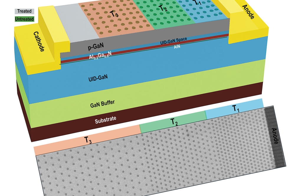
Figure 3. (a) Schematic of high-voltage lateral GaN diodes with the
plasma-based edge termination. (b) Top-view scanning electron microscopy
images of the device at different magnifications.
Unfortunately, that’s not the only modification – 10 kV-class GaN devices that have been reported usually require complicated designs, in terms of device epitaxial structure, edge termination and passivation, as well as the need for extra fabrication steps in etching, dielectric deposition, and surface treatment. That’s far from ideal, because complicated fabrication processes threaten to impair device yield and reliability, and often lead to a hike in fabrication costs.
Simplifying edge termination
Against this backdrop we are proposing a simple edge termination approach for fabricating 10 kV-class GaN power devices. What makes it simple? Well, it avoids etching and passivation processes (for an illustration of our proposed plasma-based edge termination for lateral GaN power devices on the commercial GaN HEMT platform, see Figure 2).
Eliminating etching is a significant step forward, because this process can cause surface damage, and post-treatment and passivation is often needed to alleviate detrimental device effects. Another benefit is that there’s no longer the need for precise etching, required for some of the reported 10 kV GaN devices. Precise etching is not easy, as one has to consider the thin-film thickness, film uniformity, and etching rate fluctuation. But with our approach, as well as low surface damage that comes from the absence of etching, there’s inherent passivation – so no additional passivation is needed.
Our device structure consists of a thick GaN buffer layer, an unintentionally doped layer of GaN, an AlN space layer, an AlGaN layer, another unintentionally doped layer of GaN that acts as a space layer, and p-type GaN layers. Our plasma-based edge termination is realised through conductivity tuning of the top p-GaN layer, and formation of arrays of treated and untreated p-GaN regions by a hydrogen plasma process (see Figure 3 (a)). We use a hydrogen plasma, created in a traditional inductively coupled plasma etching tool, to selectively inject hydrogen atoms into the p-type GaN layer. Once the hydrogen atom is bound to the magnesium acceptors in the p-type GaN, charge-neutral magnesium-hydrogen complexes are formed, rendering the hydrogen-plasma-treated p-type GaN highly resistive.
To assess the feasibility of our proposed plasma-based edge termination approach, we have turned to TCAD simulations. This allowed us to evaluate the impact of edge termination, employed to reduce peak electric fields and realise a more uniform electric field distribution (see Figure 4 for the simulated electric-field distributions in devices with and without our proposed edge termination).
What’s clear from our simulations is that there’s one single, large electric-field peak at the edge of the anode in the device without the edge termination. Once edge termination is introduced, so long as the conductive p-GaN layer near the anode is partially retained, there is a dramatic suppression in the peak electric field in this vicinity, leading to a more uniform electric field distribution. We have found that crucial to realising a very high breakdown voltage is optimisation of the geometry of edge termination.

Figure 4. (a) Simulated electric field mapping for the lateral GaN diodes with and without the plasma-based edge termination. The circled regions indicate high-electric-field locations. (b) The extracted electric field distribution along the cutlines in (a).
In addition to our simulations, we have fabricated and characterised devices, forming an array of circular structures, with hydrogen plasma treatment providing the edge termination of the top p-GaN layer. This involves treating the outside of the circular areas of p-GaN with a hydrogen plasma, to ensure they are resistive; and not treating the inside of the circular areas, so they retain their conductivity. Note that this difference in conductivity is visible in scanning electron microscope (SEM) images (see Figure 3 (b)).
We have investigated the performance of our diodes by adjusting various design parameters. All our devices have three array regions, designed and denoted as regions T1, T2, and T3, with increasing length LT from the anode to the cathode (see Figure 3 (b)). In each array, there are three important design parameters: the vertical spacing between each circle (ST), the lateral spacing between each circle DT, and the diameter of the circle RT. In our design, we increase ST and DT from 0.5 µm to 2 µm from region T1 to T3, while maintaining RT at 0.75 µm. These dimensions are selected to promote the distribution of the electric field – rather than crowding at the edge of the anode, the electric field is spread over the whole surface between the anode and the cathode at reverse bias. To provide a benchmark, we also fabricated a reference device, free from edge termination.
Operating under forward bias, our devices show excellent rectifying behaviour. The turn-on voltage is 1.1 V, the ideality factor is around 1.5, the on/off ratio is 1010, and the on-resistance 97 Ω mm. However, the device with the plasma-based edge termination has a current degradation of around 15 percent, due to the partially depleted 2DEG channel from the untreated p-GaN. Encouragingly, device on-resistance scales linearly with anode-to-cathode length (LAC), indicating dominant channel resistance and negligible contact resistance; and repetitive forward and backward current-voltage scans show good stability under forward bias.
Device capacitance at 0 V is 4.2 pF mm-1, and is mostly independent of LAC; and cut-off frequency is inversely proportional to capacitance and on-resistance, and increases from 0.8 GHz to 8.4 GHz as LAC decreases from 120 µm to 10 µm. We also find that as anode length (LA) increases, so does device capacitance, driving a decrease in device frequency.

Figure 5. (a) The impact of different DT on device breakdown voltages. (b) The impact of different LT
on device breakdown voltages. (c) Comparison of high-voltage lateral
GaN diodes with and without the plasma-based edge termination. (d)
Device breakdown voltage as a function of LAC with or without the plasma-based edge termination.
When we run our device under reverse bias, we are able to investigate the effects of plasma-based edge termination on device breakdown. This study has involved a simplified edge termination structure that only has region T1, and considered the relationship between the lateral spacing between circles, DT – that’s the density of the plasma treated area – and the length of region (LT).
We have determined that reducing DT – so moving to a larger circle density – helps to increase device breakdown. However, when DT is too large, there is only a minimal gain in the device’s breakdown voltage, with values comparable to those of devices without edge termination (see Figure 5 (a)). This result indicates that to ensure better electric-field management, the DT of hydrogen plasma treated regions must be small.
As part of this investigation of device characteristics under reverse bias, we have investigated the influence played by the length of region LT, considered at an LAC of 20 µm. We have found that a larger LT leads to lower device breakdown voltage, due to stronger electric field crowding at the edge of the termination structure (see Figure 5 (b)).
Finally, we fabricated 10 kV-class GaN diodes with LAC of 120 µm. Generally speaking, plasma-based edge termination increases the device average breakdown voltage by about 3 kV. We obtained a maximum breakdown voltage for a device with the plasma-based edge termination of 9.5 kV, compared with just 5.3 kV for the device without edge termination (see Figure 5 (c)). Variations in LA show minimal impact on device breakdown voltages. The relationship between the maximum breakdown voltage and LAC indicates that plasma-based edge termination provides a stronger boost for breakdown voltages at larger LAC (see Figure 5 (d)).

Figure 6. Comparison of on-resistance and breakdown voltage for state-of-the-art high-voltage GaN and Ga2O3 power Schottky diodes.
Benchmarking
We have benchmarked the performance of our device against state-of-the-art lateral and vertical GaN and Ga2O3 Schottky diodes (see Figure 6). Our diode has a Baliga’s figure of merit of 0.79 GW cm-2, comparable to that of 10 kV-class GaN and ultrawide bandgap Ga2O3 Schottky diodes.
It’s worth remembering that we have realised state-of-the-art performance with a very simple device structure, produced using simple, low-cost fabrication processes. And one should note that our edge termination technology can be transferred to other plasma-based or implantation-based fabrication processes.
In short, our work provides an alternative avenue for realising cost-effective 10 kV-class GaN power devices. To further assess the potential of our approach, we will evaluate dynamic switching performance, long-term high-voltage stability, avalanche capability, and device packaging. These investigations will increase the maturity of our technology.


