
An elegant solution for SiC
By slashing the dislocation density, solution growth promises more reliable power electronics for electric vehicles and renewable energy systems.
BY KE ZUNBIN, QIAN HAO, YIN ZURONG, WANG HAN, SHI ZHIJIE, HU JIANTAO AND LU MIN FROM CHANGZHOU PERFECT CRYSTAL SEMICONDUCTOR AND SHI TIANLE FROM THE UNIVERSITY OF SHANGHAI FOR SCIENCE AND TECHNOLOGY
There’s little debate surrounding the darling of the power electronics world. It’s SiC, a remarkable material that keeps electric vehicle motors spinning efficiently, ensures a smooth power flow in smart grids, and prevents data centres from overheating under immense computational loads. Its secret lies in its unique combination of assets: the thermal conductivity of copper, the breakdown strength of diamond, and the ability to handle voltages that would fry ordinary silicon chips.
But beneath this glittering reputation lurks a microscopic menace. The crystal defects that chipmakers struggle to eliminate – known as dislocations – hold back device performance and reliability. Today’s commercial SiC substrates are riddled with these atomic-scale imperfections, with thousands threading through each square centimetre of material. Every one of them acts as a tiny electron trap, sapping efficiency and providing a pathway for destructive current leakage. For engineers designing the next generation of high-power systems, these defects are a critical bottleneck.

Table 1. Effects of SiC dislocations on different devices (for more details, see Nanoscale Research Letters 17 30 (2022). Note: VB is blocking/breakdown voltage; Ron is on-resistance; Ileak is leakage current; Iop is operating current; τ is carrier lifetime.
Fortunately, help is at hand. While the mainstream semiconductor industry continues to focus on physical vapour transport – the established but imperfect method for growing SiC crystals – researchers are refining an alternative approach that could leapfrog current limitations. It’s solution growth, a technique that crystallises SiC from a molten metal bath rather than from vapour – and it’s demonstrating an unprecedented ability to purge these troublesome dislocations.
Leading the way is our team at Changzhou Perfect Crystal Semiconductor, supported by the University of Shanghai for Science and Technology. Working together, we have systematically unpicked the mechanisms of dislocation behaviour during solution growth, revealing how to optimise this process and produce crystals of remarkable purity.
Our findings point to a future where SiC wafers contain not thousands of dislocations per square centimetre, but merely hundreds. For device manufacturers, that means more efficient power converters, more reliable motor controllers, and ultimately, cheaper renewable energy.

Figure 1. The transformation dance, with threading dislocations in an
off-axis seed crystal converted into basal plane defects as macrosteps
flow across the growth surface. These defects glide sideways and exit
the crystal, dramatically reducing defect density in the final wafer.
The enemy within
To appreciate the challenge in making a breakthrough, one must first understand the adversary. This comes in three forms, each with a different personality. There are: threading screw dislocations, spiralling through the crystal-like microscopic corkscrews; threading edge dislocations, creating atomic mismatches along their path; and Basal plane dislocations, slipping along the crystal’s natural layering planes. All act as trap centres – electronic black holes that capture charge carriers and waste energy, lost as heat.
These dislocations have stark consequences. In MOSFETs, the workhorses of power conversion, these imperfections increase resistance and degrade the fragile gate oxide. In Schottky barrier diodes, they hike leakage currents. And in bipolar devices, they shorten carrier lifetimes. As illustrated in Table 1, every major device type suffers. Since commercial substrates contain between 10³ and 10⁴ dislocations per square centimetre, device manufacturers take a yield hit.

Figure 1. The transformation dance, with threading dislocations in an off-axis seed crystal converted into basal plane defects as macrosteps flow across the growth surface. These defects glide sideways and exit the crystal, dramatically reducing defect density in the final wafer.
Traditional crystal growth methods struggle to reduce defect densities below this range. Physical vapour transport, which sublimates SiC powder at over 2,300 °C before recondenses it as a crystal, inevitably introduces thermal stresses that generate fresh dislocations. Switching to high-temperature CVD ensures better control, but uses hazardous gases, and is prohibitively expensive for bulk crystal production. With both approaches hitting a quality ceiling, the power electronics industry is desperate for a solution – in fact, it has been wanting one for a number of years.
A superior solution
Solution growth takes a fundamentally different approach. It involves immersing a seed crystal in a molten solution of silicon, mixed with metals such as chromium and aluminium. A dash of chromium dramatically boosts carbon solubility, while aluminium smooths the growth surface. Using a modest temperature gradient of around 1,800 °C, which is significantly cooler than vapour methods, carbon atoms precipitate onto the seed, steadily assembling a high-quality crystal.
The advantages of solution growth are not limited to lower run temperatures. Additional benefits include a natural suppression of micropipes, the giant screw dislocations plaguing vapour-grown crystals. More intriguingly, solution growth actively converts problematic threading dislocations into less harmful forms, and can even sweep them entirely out of the crystal (see Figure 1). It’s this transformative capability that we set out to understand and optimise.

Figure 3. Temperature matters. Dislocation density maps of wafers grown under different thermal gradients. (a) A steep 5 °C cm-1 gradient produces high defect counts. (b) Reducing the gradient to 2 °C cm-1 slashes dislocations by minimising thermal stress that generates fresh defects.
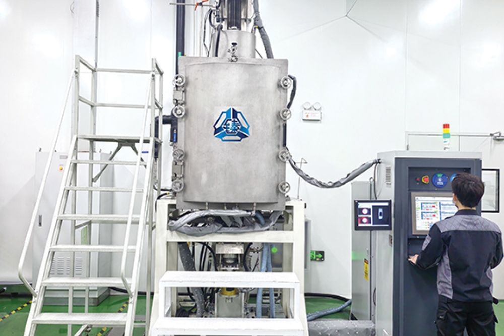
Our experiments, conducted in a bespoke resistance furnace (see Figure 2), have focused on the systematic variation in key growth parameters. Using 6-8-inch 4H-SiC seed crystals – that’s the industry standard polytype – we have grown crystals for 50 hours under controlled conditions.
Each of these crystals has been sliced, polished, and etched to reveal its defect structure under optical microscopy. Results provide a clear path to defect suppression.
The first breakthrough has come from temperature control. In solution growth, a temperature gradient at the growth interface drives the process, but excessive gradients spell trouble. When we
pushed the gradient to 5 °C per centimetre, dislocation densities soared. Dialling this gradient back to 2 °C per centimetre slashed defects dramatically (see Figure 3). The mechanism behind this improvement is straightforward: thermal stress, induced by steep gradients, generates new dislocations upon relief. Moving to gentler gradients allows the crystal to relax, preserving its structural integrity.
We have found that the moment of seeding is even more critical. When a cold seed crystal first touches a hot solution, there’s a sudden shock, threatening to generate thousands of new dislocations.
However, by pre-heating the seed just 5 mm above the solution surface – giving it a modest 3 °C temperature boost – we quash this thermal shock by half compared with a 10 mm stand-off distance. Thanks to just this simple procedural tweak, we are cutting the dislocation generation at the crystal’s foundation, and influencing the quality of everything that grows above (see Figure 4).
Pores are a second significant defect source. These gas bubbles, trapped between seed and solution, interrupt growth and spawn dislocations. We have identified two culprits: surface misalignment during seeding, and dissolved gases precipitating from solution.

Figure 4. The shock of contact. Preheating the seed crystal close to the
solution surface minimises thermal shock. (a) Baking the seed 5 mm
above the solution, creating only a 3 °C temperature jump, yields far
fewer dislocations than (b) a 10 mm stand-off with a 6 °C shock.
Some of the pores are quite large, with dimensions of up to two millimetres. One of their downsides is that they create circular dead zones, where no growth occurs. But that’s not the only issue – the surrounding crystal is rough, with solvent inclusions, causing nearby dislocation counts to skyrocket (see Figure 5). Equally damaging, while less visually dramatic, are smaller pores. We found that in a region with micron-scale pores, there were 628 threading dislocations in the microscope’s field of view, versus just 172 in a pore-free region – that’s a fourfold increase (see Figure 6).
The solution is meticulous process control. It’s possible to all but eliminate pore formation by ensuring parallel contact between seed and solution, optimising furnace pressure, and thoroughly dissolving any surface corrosion pits on the seed. Do all of this, and a smooth, uninterrupted growth front follows that doesn’t generate fresh dislocations.

Figure 5. When pores strike. (a) A crystal containing large
millimetre-scale pores that interrupt growth. (b) A wafer sliced through
such a pore shows a circular dead zone surrounded by rough,
inclusion-rich crystal.
The expansion advantage
Perhaps our most valuable finding concerns diameter expansion. We have found that a remarkably effective approach to purging defects is to start with a small seed crystal, and gradually widen the crystal as it grows. Note that in the expansion region, the growth direction tilts relative to the threading dislocation lines, encouraging them to bend into the basal plane and exit through the crystal edge. In some experiments, we observed complete elimination of dislocations in the expansion region (see Figure 7).
This finding stands in sharp contrast to conventional on-axis growth, where threading dislocations propagate straight upwards, locked parallel to the growth direction. So, we can conclude that the solution method’s inherent ability to control crystal shape becomes a powerful defect-filtration mechanism – a trick that vapour-phase methods struggle to replicate.
Another leaver for control is the orientation of the seed crystal. When growth proceeds on a precisely on-axis (0001) seed, this suppresses basal plane dislocations, which cannot easily propagate vertically. However, this geometry does nothing for threading dislocations, which sail straight through (see Figure 8).
The game-changer is a 4 ° off-axis seed, tilted toward the <1120> direction. A stepped growth surface results, where macrosteps continuously flow across the crystal. Intersecting these steps are threading screw and edge dislocations. Basal plane defect steps result, which then glide laterally out of the crystal. Using this approach, we deliver dramatic reductions in threading dislocation density compared with the original seed crystal (see Figure 9).

Figure 6. Micropores, macro impact. (a) A crystal with micro-pores that
closed early, leaving a smooth surface. (b) Edge micro-pores visible in
cross-section. (c) Dislocation density in a clean region: 172 threading
defects in view. (d) Near pores, this jumps to 628 – a fourfold
increase.
From lab to fab
What do our improvements mean in practice? Our optimisation – gentle temperature gradients, pore elimination, diameter expansion, and off-axis seeding – work synergistically. While we have not reported a single combined figure from these approaches, individual improvements are substantial: cutting the temperature gradient from 5 °C to 2 °C per centimetre reduces thermal stress by more than half; eliminating pores prevents a four-fold spike in dislocations observed near bubble traps; diameter expansion enables local dislocation densities of zero; and off-axis seeding transforms the majority of threading dislocations, realised within the first few millimetres of growth.
Such success will pique the interest of device manufacturers, as it translates into higher production yields and better performance. Transformative gains may result, such as the difference between a power MOSFET that operates reliably at 200 °C, and one that fails prematurely. A step change in dislocations could also enable Schottky diodes to block higher voltages without leakage, and open the door to IGBTs with longer carrier lifetimes for more efficient switching.

Figure 7. Expansion eliminates defects. (a) In the diameter expansion
region, dislocation density drops dramatically as threading defects bend
and exit the crystal. (b) The original seed region retains higher
defect densities.
Implications extend well beyond individual devices. As electric vehicles move toward 800 V architectures for faster charging, demand for ultra-low-defect SiC is intensifying. Magnifying this demand are: solar inverters and grid storage systems, operating at megawatt scales, that value incremental efficiency gains; and data centres, where power conversion losses account for a significant fraction of electricity consumption, and superior SiC trims operating costs and cuts carbon footprints.

Figure 8. On-axis limits. (a) Dislocation map of an on-axis seed
crystal. (b) After growth, threading dislocation density remains
similar, though basal plane dislocations are suppressed.
Like many new technologies, while there’s promise, challenges are still to be addressed. One is the growth rate, which remain slower than vapour transport, but the gap is narrowing. Another is scaling to 12-inch wafers – the next industry target – a goal that demands careful engineering of thermal fields and fluid dynamics; and there is also the requirement for recycling, to keep costs competitive. Yet the fundamental advantages are compelling: lower temperatures, lower defect densities, and lower material costs.
Through Changzhou Perfect Crystal Semiconductor, we are now commercialising our technology, offering 6-12-inch solution-growth furnaces and low-resistivity p-type substrates – a speciality that remains difficult for physical vapour transport.

Figure 9. Off-axis advantage. (a) Starting seed with moderate defect
density. (b) After growth on a 4 ° off-axis seed, threading dislocation
density plummets as macrosteps convert them to basal plane defects that
exit the crystal.
The road ahead involves integrating our insights into automated production systems. Through the introduction of real-time monitoring of growth interfaces, AI-driven process control, and advanced seed preparation techniques, we will push dislocation densities to new lows. We anticipate commercial substrates with fewer than 500 dislocations per square centimetre – a quality level that today seems aspirational. For the power electronics industry, our message is clear. The SiC revolution is just beginning, with solution growth poised to deliver a hike in crystal quality that next-generation applications demand.


