Combining a CMOS driver and a GaN power switch on 300 mm silicon
Intel’s DrGaN technology, involving the monolithic integration of GaN and silicon CMOS on 300 mm wafers, will support power delivery in tomorrow’s data infrastructure and communication networks.
BY HAN WUI THEN FROM INTEL CORPORATION
The number of power-hungry applications involving massive computation is on the rise, due to growth in datacenters, AI, wafer-scale compute, supercomputers and 5G/6G networks. Due to this, there is a need for the ICs that power these applications to combine a superior level of performance with greater energy efficiency and higher densities.
Our team at Intel Technology Research has anticipated these trends and has already devoted many years to addressing them. Back in 2019 we developed the industry’s first enhancement-mode (E-mode) GaN transistor, enabled by high-k dielectric metal gate technology; and we pioneered monolithic three-dimensional stacking integration of GaN and silicon transistor technology, all using 300 mm silicon wafers. During these efforts, we pursued the use of GaN because this high-mobility wide-bandgap semiconductor can operate at high frequencies and high power densities. These assets make this particular technology the best-in-class for power delivery and RF applications. We have focused on combining the advantages of GaN and silicon CMOS on a single chip to realise best-in-class performance, high efficiency and high density (small form-factor), as well as to integrate functionalities beyond what is possible with an n-channel only GaN technology.

Figure 1. (a) A typical state-of-the-art solution involves a co-packaged two-die implementation: a separate CMOS driver die and power GaN die, where the driver signal from the CMOS die is routed through the package (represented by parasitic inductance, L) to the power GaN die. One downside of this approach is that it causes extreme ringing, visible in the simulation (inset). (b) A new approach facilitated by DrGaN, with a fully integrated CMOS driver on the power GaN die, enables a low-inductance path from the CMOS driver output to the GaN power switches. This technology suppresses the large ringing in (a).
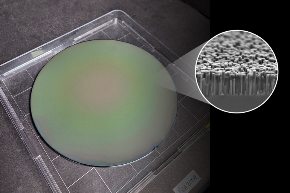
Recently, we have taken our research a step further, employing an improved version of this process. At the most recent International Electron Devices Meeting, held last December in San Francisco, we unveiled what we refer to as ‘DrGaN’: it is a large-scale integrated CMOS driver-GaN power switch technology, realised on a 300 mm GaN-on-silicon wafer.
A single die solution
Our DrGaN technology breaks new ground. It is the first time that a GaN power transistor technology has been enhanced with an integrated CMOS driver on the same die. In comparison, other state-of-the-art GaN technologies of today employ a separate CMOS driver die that accompanies a GaN die, with the driver signal from the CMOS die routed through the package to the GaN die. This routing through the package incurs parasitic inductance (see Figure 1(a)), which limits performance, with extreme ‘ringing’ at high switching speeds (this is visible in the simulation trace, shown in the inset of Figure 1(a)).

Figure 2. Benchmarking the power figure-of-merit (RONxQGG) of the GaN transistor of this work shows: a performance that’s around a 20-fold better than the pGaN HEMT and around a 30-fold better than silicon LDMOS at 40 V; a 10-17-fold better performance than silicon LDMOS and a pGaN HEMT at 12-15 V, and 7-fold better performance than a silicon finFET at 5 V.
This ringing is detrimental, limiting the switching speed and the performance, in terms of the conversion efficiency. Due to this ringing, it’s not possible to exploit a key advantage of the GaN transistor, which can switch far faster than its silicon sibling, evidenced by a figure-of-merit around 10-20 times higher (see Figure 2).
In addition, pairing a GaN die with a CMOS die leads to voltage ‘overshoot’. Two issues result from this: an increase in the stress subjected to both the CMOS and GaN transistors; and inadvertent activation of the GaN power switch during the off-interval.

Figure 3. The process flow used for DrGaN technology, which involves
three-dimensional monolithic integration of GaN and silicon CMOS by
layer transfer on 300 mm silicon wafers.
There is no doubt that a two-die solution fails to realise the full potential of the figure-of-merit gains offered by GaN. Overcoming this limitation is our DrGaN technology. By offering a fully integrated CMOS driver on the GaN die, our approach enables the realisation of a low-inductance path from the driver output to the GaN power gate, thereby suppressing the substantial ringing. The upshot is higher frequency operation, alongside a higher efficiency and improved reliability. The higher switching frequencies are cherished, as they open the door to smaller passives, such as smaller inductors. Shrinking the size of the power delivery unit follows, enabling higher power densities – that is, power delivery occupies less space-per-unit-power delivered, while maintaining high performance. Note that what we have just described is an instance of Moore’s law in action for the power delivery solutions provided by DrGaN technology.

Figure 4. (a) Intel’s prior work involved the three-dimensional
sequential monolithic integration of GaN and silicon CMOS by a layer
transfer process, with silicon PMOS/NMOS transistors fabricated after
completing fabrication of the GaN transistors. (b) For Intel’s latest
work, DrGaN technology, GaN and silicon PMOS/NMOS transistors are
fabricated in such a way that the high-temperature activation steps are
completed before the deposition of the gate dielectric of the GaN
transistors.
Our company has a long and strong track record in driver and MOSFET integration. Back in 2004 we introduced ‘DrMOS’ – driver and MOSFET integration for the silicon MOSFET. Our motivation for this breakthrough came from the need to keep pace with increasing microprocessor power density and efficiency demands associated with the leading PCs and laptops of that era. Since then, DrMOS has become the gold standard for point-of-load power delivery solutions for CPUs and GPUs.
One of the trailblazers for GaN is Navitas Semiconductor, which introduced integrated enhancement-depletion (E-D) mode n-channel drivers for high-voltage GaN power ICs. This particular architecture has been adopted because standard GaN processes cannot produce p-channel or CMOS devices.

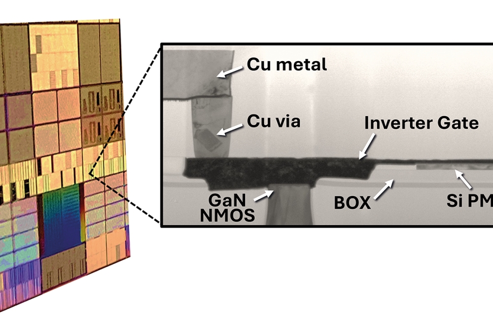
Figure 5. Transmission electron microscopy of the completed (a) GaN
transistor, (b) silicon PMOS transistor and (c) CMOS inverter,
fabricated in this process on a 300 mm wafer.
The E-D mode driver is suitable for high-voltage scenarios. However, this form of driver is far too leaky – and thus not efficient enough – for lower voltage, point-of-load applications, such as those below 48 V. Turning to CMOS addresses this, while enabling efficient, high-density integration of other functionalities, including control logic and telemetry circuitries, such as current and temperature sensors. It is a broad range of features, challenging to realise with a standard GaN n-channel only process.
With our DrGaN technology, we accomplish the monolithic integration of GaN and silicon CMOS with a new process flow (see Figure 3), using a technique called layer transfer. We begin by bonding a donor silicon wafer to a GaN wafer. Upon separation, the silicon donor wafer cleaves along a weakened crystal plane throughout the wafer, to leave a thin layer of silicon channel material bonded onto the GaN wafer.
Our latest approach involves introducing implants and high-temperature activation steps, for the fabrication of the silicon CMOS transistors, prior to formation of the high-κ gate dielectric of the GaN transistors. From there onwards, we only perform low-temperature steps. That’s critical, because high temperatures threaten to degrade the quality and reliability of the high-κ gate dielectric used for GaN transistors. By arranging our process flow in such a manner, this truly gate-last process overcomes a major hurdle in three-dimensional monolithic integration of GaN NMOS and silicon CMOS transistors.

Figure 6. The current-voltage (I-V) characteristics of (a) GaN
transistor, and a (b) silicon PMOS transistor produced by the DrGaN
process.
Proven superiority
The benefits of our latest process are seen in the measurements of silicon PMOS transistors fabricated by both approaches (see Figure 4). Previously, PMOS transistors were fabricated sequential, only after the GaN transistors were completed. This sequence exposed the gate dielectric of the GaN transistor to the high-temperature steps of silicon transistor processing.
Another downside of our previous approach is that this sequential process flow employed intra-connects to establish electrical connectivity between the silicon and GaN transistors. As well as necessitating additional fabrication steps and masks, these intra-connects added path resistance when accessing the underlying GaN transistors. In contrast, our latest process for producing GaN and silicon CMOS transistors leads to a shared backend copper interconnect stack, eliminating the need for additional intra-connects and masks.
To inspect our completed devices – the GaN transistor, silicon PMOS transistor and hybrid GaN/silicon CMOS inverter – we have used a transmission electron microscope (see Figure 5). These devices, fabricated with our latest process on a 300 mm wafer, are used to construct the DrGaN.

Figure 7. (a) The figure-of-merit 1/(RONQGG) for the GaN transistors produced by the DrGaN process, for channel lengths, LG, ranging from 30 nm to 250 nm. (b) The on-resistance, RON, and breakdown voltage, BVDS, for GaN transistors produced by this process. Gate-to-drain lengths, LGD, are between 200 nm and 1000 nm.
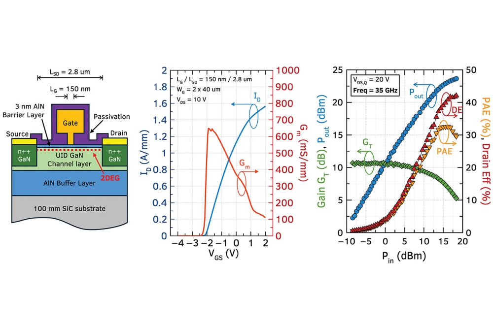
We have undertaken a number of electrical measurements on our devices. Transfer current-voltage (I-V) characteristics for a typical GaN transistor with a channel length of 90 nm are shown in Figure 6 (a). Strengths of this device include an excellent on-off ratio of around 1010, a low on-resistance of 422 Ω µm, a high drain-current drive of 1.2 mA µm-1, and gate leakage below 1 pA µm-1. Equally impressive are the I-V characteristics of our silicon PMOS transistor, which has a channel length of 180 nm (see Figure 6(b)). In this case the on-off ratio is around 106, the on-resistance 1780 Ω µm, the drain current drive 0.43 mA µm-1, and the gate leakage around 1 pA µm-1. Note that these are some of the best numbers ever reported for GaN and silicon PMOS transistors at comparable channel lengths. In particular, the GaN transistors show a best-in-class figure-of-merit for the reciprocal of the product of on-resistance and gate charge of 0.59 mΩ-1 nC-1, measured from the shortest channel length of 30 nm (see Figure 7).
Through judicious selection of gate-to-drain separation, which can be varied from 200 nm to 1000 nm, we can obtain a breakdown voltage of up to around 60 V for our GaN transistor (see Figure 7). This enables us to target a range of use cases and application voltages.

Figure 8. The layout of a 40 µm by 10 µm DrGaN unit cell consisting of
silicon PMOS and GaN NMOS driver blocks, and two GaN power switch
transistor blocks. The inset shows the circuit schematic of the
electrical connections between the silicon PMOS, GaN NMOS and GaN power
switch transistors. In the driver block, the silicon PMOS has a channel
length, LG, of 180 nm, and a total width per unit cell of
19.76 µm, while the GaN NMOS has the same channel length of 180 nm and
total width-per-unit-cell of 36 µm. The GaN power switch transistors
have a similar channel length of 180 nm, but a larger total
width-per-unit-cell of 306 µm, and a longer gate-to-drain length, LGD, of 400 nm, in order to withstand a higher operating voltage.
Our DrGaN technology enables the construction of a large-scale IC from a massive array of repeated unit cells. Each of these cells, 40 µm by 10 µm in size, consists of four blocks: a silicon PMOS driver block, a GaN NMOS driver block, and two symmetrical GaN power switch blocks. The layout for these cells is outlined in Figure 8, along with a circuit schematic that illustrates the electrical connections between the silicon PMOS, GaN NMOS and GaN power switch transistors.
The DrGaN unit cell is arrayed over an area of 0.8 mm2 to realise a desired total width of 421.1 mm for the GaN power switch, 49.54 mm for the GaN NMOS (driver) and 27.19 mm for the silicon PMOS (driver). The aggregate total width of all the transistors is 497.83 mm.
To demonstrate the full functionality of this 497.83 mm wide DrGaN, we have measured its steady-state electrical characteristics. To record the transfer characteristics of the GaN power switch S, which has a total width of 421.1 mm, in DrGaN, we use a probe to apply a bias voltage to the gate node of this switch (see Figure 9(a)). For this GaN power switch we have measured an on-resistance of 1 mΩ and determined leakage characteristics, with the switch turned off by applying a bias voltage of either (c) 0 V directly at the gate node of S; or (d) 1.8 V at the gate driver node of P and Q. Drain and gate leakage currents are well below 0.1 mA for the 421.1 mm-wide power switch. Also shown in Figure 9 are the transfer characteristics of silicon PMOS, P (width of 27.19 mm) (e) and the leakage characteristics of GaN NMOS, Q (width of 49.54 mm), in the gate driver (f).
We have also assessed the inverting characteristics of the combined GaN-silicon CMOS driver (P and Q). Figure 10 shows the steady-state transfer characteristics with DrGaN. Modulation of the GaN power switch, S, is driven by the integrated GaN-silicon CMOS driver (P and Q).

Figure 9. (Top) the transfer characteristics of the GaN power switch S
with a total width of 421.1 mm in DrGaN, demonstrating transistor
operation. The normalized RDSON is 0.8 mΩ mm2. (Middle) The leakage characteristics, ID-IG-VD and ID’-IG’-VD of the GaN power switch S in DrGaN, in the off-state accomplished by either applying a bias voltage, VG,
of (c) 0 V directly at the gate node of S; or (d) 1.8 V at the gate
driver node of P and Q. (Bottom) The I-V transfer characteristics of the
(e) silicon PMOS, P, and (f) GaN NMOS, Q, in the gate driver of DrGaN.
This final measurement completes full functionality testing of our DrGaN technology, which has multiple merits. We view our realisation of a large-scale, 497.83 mm-wide DrGaN is an important milestone towards demonstrating the viability of our 300 mm GaN-on-silicon process with three-dimensional monolithically integrated GaN and silicon CMOS, brought together by layer transfer. Our efforts break new ground, showing for the first time that this process can produce large-scale integrated circuits comprising GaN and silicon CMOS transistors on the same chip.

Figure 10. (Top) Transfer characteristics, Vout-Vin,
of the GaN-silicon CMOS driver, P and Q, in DrGaN technology. (Bottom)
The steady-state transfer characteristics of DrGaN. The switching of the
GaN power switch, S, is driven by the integrated GaN-silicon CMOS
driver (P and Q). Turning on involves a driver pull-up to a VG rail of 1.8 V, and turning off involves a driver pull-down to a VG rail of 0 V.
Our development of DrGaN demonstrates that the monolithic three-dimensional integration of GaN NMOS and silicon PMOS transistors is a powerful way to integrate two dissimilar best-in-class semiconductor technologies on the same silicon and deliver optimal performance, improved density, and more functionalities. Our accomplishments include the industry’s first CMOS DrGaN technology fabricated in 300 mm GaN-on-silicon technology. Through the use of enhancement-mode high-k dielectric GaN MOSHEMT technology for the GaN transistor, our DrGaN ICs set new benchmarks for performance and leakage. Another significant advance is the new improved truly gate-last process flow, resolving a major hurdle in three-dimensional monolithic integration of GaN NMOS and silicon CMOS transistors.
Thanks to our efforts, there has been a significant advance in 300 mm GaN-on-silicon technology. But that’s far from all that the demonstration of DrGaN has accomplished. This technology holds the key to tomorrow’s efficient, highly integrated, high-density point-of-load power delivery solutions for future high-performance compute in datacenters, AI and 5G/6G networks. DrGaN is clearly destined to deliver many great things.
The author, Han Wui Then, would like to thank team members and contributors:
M. Radosavljevic, S. Bader, A. Zubair, H. Vora,
N. Nair, P. Koirala, M. Beumer, P. Nordeen,
A. Vyatskikh, T. Hoff, J. Peck, R. Nahm,
T. Michaelos, E. Khora, R. Jordan, C. Hoffman,
N. Franco, A. Oni, S. Beach, D. Garg, D. Frolov,
A. Latorre-rey, A. Mitaenko, J. Rangaswamy,
S. Sarkar, S. Ahmed, V. Rayappa, H. Chiu,
A. Hubert, S. Brophy, N. Arefin, N. Desai,
H. Krishnamurthy, J. Yu, K. Ravichandran, and
P. Fischer.