EU to help establish PIC pilot line

The EU's Chips Joint Undertaking (Chips JU) has selected the consortium with which it will start negotiations to establish the Advanced Photonic Integrated Circuits (PIC) pilot line for Europe - PIXEurope.
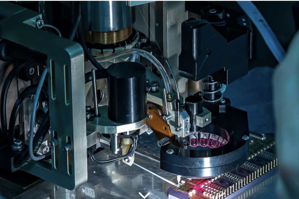
PIXEurope will use state-of-the-art equipment to develop innovative PIC technologies and processes, including design, chip fabrication and hybrid integration, through to packaging, test and reliability technologies. The location is expected to be in the Netherlands.
The Pilot Line will be jointly funded by the European Union, through the Horizon Europe and Digital Europe Programmes, Participating States, and private organisations. A total of €380 million (~$405 million) has been allocated for the project, with €133 million expected to be invested in the Netherlands.
Coordinated by the Institute of Photonic Sciences, the 20-member consortium includes participants from Spain, Ireland, the Netherlands, Finland, Belgium, Portugal, Poland, Austria, Italy, France, and the United Kingdom.
The PIC pilot line is the fifth pilot line to be implemented in Europe by the Chips JU to strengthen the continent’s semiconductor ecosystem. Aligned with the goals of the Chips for Europe Initiative, the PIC pilot line is expected to collaborate closely with the other four Chips JU pilot lines, design platform, and competence centres.
Jari Kinaret, Chips JU executive director, emphasised the importance of this Pilot Line: “This selection is an important step for the semiconductor industry and Europe’s capacity in the production of photonic integrated circuits. We are looking forward to the negotiations with the selected consortium.”