Could BN replace GaN?
China produces nearly 98 percent of the world’s supply of semiconductor gallium, according to the US Geological Survey. In response to the country’s move to limit exports on the compound, the US Department of Energy (DOE) put out a call for proposals to US scientists to engineer a solution to replace GaN-based semiconductors and awarded four teams $1 million for a one-year research sprint.
Patrick Lenahan, a professor of engineering science and mechanics at Penn State, will investigate the possibility of replacing GaN-based devices with boron nitride. Co-principal investigators from the Ohio State University, the University of Iowa and QuantCAD — a quantum technology start-up with locations in Iowa City, Iowa, and Chicago — will join Lenahan in the investigation.
“We believe boron is a potentially good alternative to gallium in some technologically critical GaN-based applications, but we don’t know exactly how this may work out,” Lenahan said. “Our team, which involves theorists and experimentalists, will work to determine how boron nitride works, physically, in systems of real interest, and what could be the potential drawbacks in using it in place of GaN.”
Boron nitride has comparable, but far less understood, physical characteristics to GaN, and may have the potential to perform similarly in some critical applications. “Boron does not have the same importation restrictions as gallium, so it could be a long-term replacement in multiple applications,” Lenahan said.
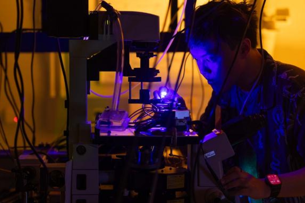
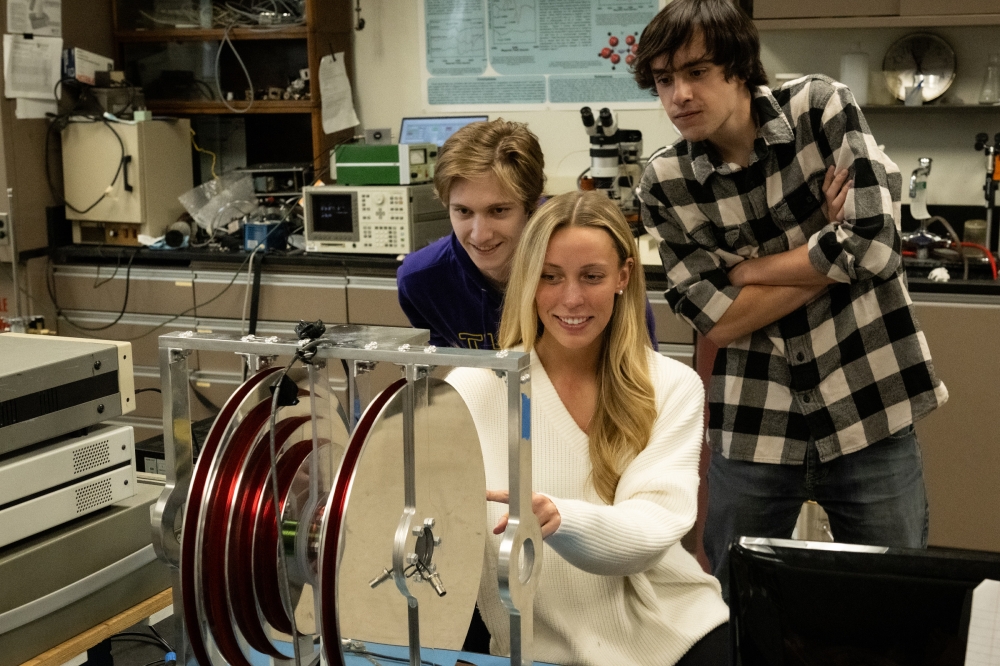
Lenahan and the students in his lab will use techniques — such as electrically detected magnetic resonance, near zero field magnetoresistance and conventional electron paramagnetic resonance in conjunction with a variety of electrical measurements — to assess semiconductor devices manufactured with boron nitride. All three techniques provide information about the ways electrons interact with imperfections in boron nitrides by testing a property of electrons called spin. Such understanding will be key in evaluating boron nitride’s effectiveness as a semiconductor, Lenahan said.
“This project is very much a team effort, involving device fabrication, a variety of measurements and theoretical analysis,” he added.
Ezekiel Johnston-Halperin, professor of physics and co-director of the Center for Quantum Information Science and Engineering at Ohio State, will fabricate devices built up from 2D layers of boron nitride and explore electronic transport through a process called electron tunneling.
Johnston-Halperin's lab has piloted a process for building very thin structures that take advantage of electron tunnelling to sensitively probe the properties of atomic impurities in boron nitride. "By picking a thickness for boron nitride just beyond the range of this tunnelling process, the current through the device becomes extremely sensitive to the presence of crystalline defects,” he said.
Lenahan and Johnston-Halperin, along with Sina Soleimanikahnoj from QuantCAD and Durga Paudyal, a researcher from the University of Iowa, will work together to obtain a unique “fingerprint” of impurities in boron nitride in order to optimise the design of the compound’s chemical structures.
With the tight timeline on this one-year research sprint, the collaborators will work in tandem to establish whether a realistic path forward exists for boron nitride and to broadly determine how scientists and technologists could most effectively proceed on this path.


