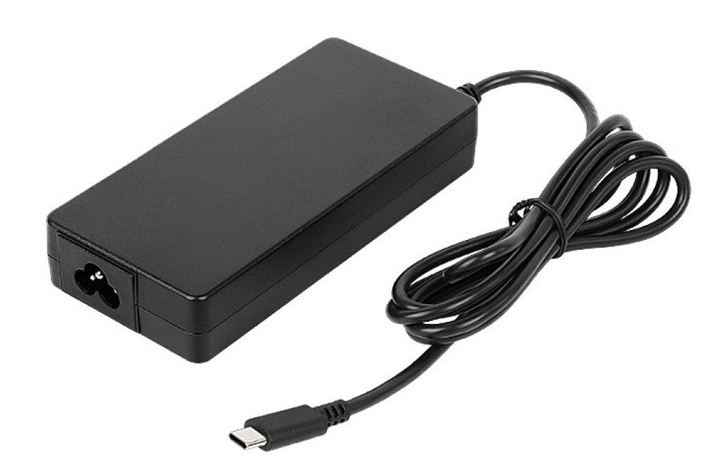
AKM starts shipping smallest Hall element
Asahi Kasei Microdevices (AKM) has launched mass production and shipment of its next-generation InAs compound Hall element, the HQ0A11.
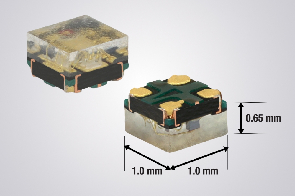
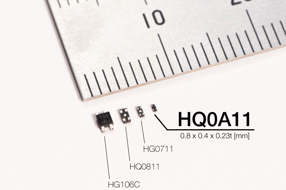
Launched in November 2024, HQ0A11 features AKM's smallest and thinnest package size for an InAs-based Hall element, measuring 0.8 x 0.4 x 0.23 mm. It achieves an 85 percent reduction in volume compared to the previous model of HQ0811 in the high-sensitivity HQ series. It is expected that HQ0A11 will contribute to improved performance in smartphone camera modules, small robots, and other applications.
HQ0A11 is smaller and thinner than the HQ0811 (1.6 x 0.8 x 0.38 mm), which was previously the smallest and thinnest high-sensitivity Hall element. It also has an approximately 16 percent better S/N (signal- to-noise) ratio, which directly correlates to position detection accuracy, than HQ0811, which previously had the highest S/N performance in the HQ series.
Hall elements are often used for the position detection that is needed for image stabilisation and autofocus in smartphone cameras. The demand for enhanced functionality and higher-resolution capture in cameras requires an increased component count within the same (or smaller) form factor, creating a growing need for ultra-compact products that enable high-density component mounting in a limited space.
HQ0A11 is said to achieve the highest S/N performance among AKM products for position detection by leveraging the characteristics of InAs. Its position detection accuracy is over 3.5 times higher than that of the HG0C11, a GaAs Hall element which has been a mainstay product for camera modules. As such, HQ0A11 can significantly reduce the lens-shake effect that often occurs with smartphone cameras, especially with telephoto lenses.