Aledia's microLED line is ready to roll

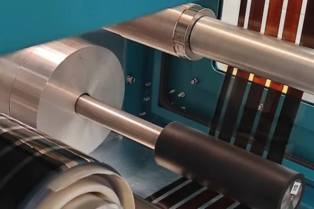
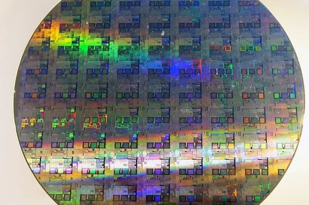
At CES 2025, French microLED display firm Aledia has announced that its $200m state-of-the-art microLED production line in Grenoble is ready to support customer demand ramp-up to nearly 5,000 wafer starts per week..
After 12 years of research, a portfolio of nearly 300 patents and $600 million in investment, Aledia believes its microLED-based microdisplay – with Red, Green and Blue microLEDs on the same substrate - can solve the toughest hardware challenges for AR, paving the way for the most immersive, AI-powered AR vision experiences to date.
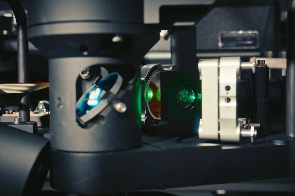
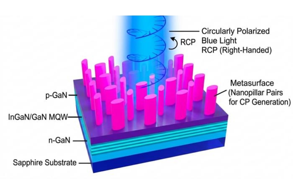
The 3D GaN-on-silicon nanowire technology is said to offer higher brightness and better energy efficiency than 2D LEDs, with the 3D structure allowing for precise and directive light emission, suiting it to applications like AR.
“Immersive technologies such as AR haven’t reached their full potential as the industry has yet to design screens that are both slick and highly functional,” said Pierre Laboisse, president and CEO of Aledia. “At Aledia, we’ve created a nanowire technology that makes microLED displays thinner, more power efficient and easier to produce for mass adoption. By next CES, OLED and LCOS will already be phased out in favour of our superior microLED technology.”
“Our Champagnier factory is a key milestone for European innovation, and we are proud to represent it at the Auvergne Rhône-Alpes Pavilion at CES,” added Laboisse. “We are redefining global standards of display technology with our efficient and high-performing chips, positioning Grenoble as the global center of microLED production.”