Photon IP raises €4.75m for advanced PICs

Photon IP, a Netherlands-based maker of optical chips, has raised €4.75 million in a seed round led by Innovation Industries with participation from Faber and Brabantse Ontwikkelings Maatschappij (BOM) and with funding support from PhotonDelta.
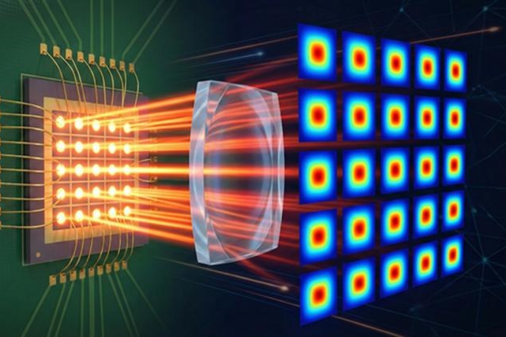
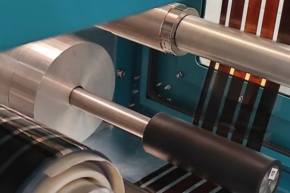
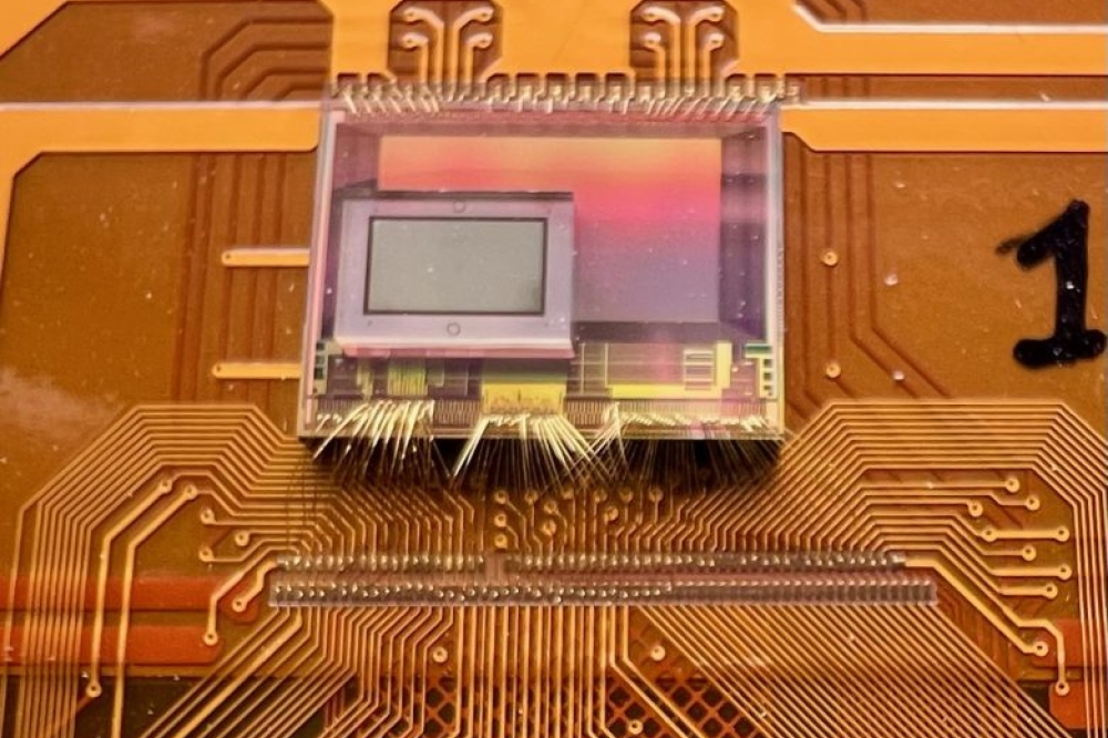
With this financing, PHOTON IP plans to accelerate the industrialisation and commercialisation of its technology, which is designed to efficiently combine silicon photonics with active III-V materials.
Communication networks, data centres for AI and advanced sensing applications are all dependent on optical chips, and the technologies available to more efficiently integrate multiple materials are becoming a fundamental barrier. Photon IP says its technology addresses this challenge by reinventing the way silicon and different III-V materials, such as InP are integrated.
“We’re not just advancing integrated photonics – we’re simplifying the manufacturing process for photonic circuits as well,” said Photon IP co-founder and CEO Rui Santos. “With our advanced optical engines, we’re setting a new performance benchmark and eliminating the barriers to efficiently combining III-V materials with silicon. This funding expands our ability to grow our team and bring our first products to market.”
Vincent Kamphorst, investment director at Innovation Industries, said: “We are excited to announce our investment in Photon IP. By effectively coupling diverse photonic platforms in a mass-manufacturable process, the company aims to deliver high-performing photonic solutions at volume. We look forward to supporting Photon IP as they develop.”