MIT spin-out CDimension reveals early customers
CDimension, an MIT spin-out developing a wafer-scale process for synthesising 2D semiconductors such as MoS2 snd WSe2, has announced that US research institutions Carnegie Mellon University, Duke University, and UC San Diego are its first early-stage university customers.
“Bringing 2D materials from the lab to real-world applications requires reproducible, high-quality films that can scale across full wafers,” said Xu Zhang, associate professor of electrical and computer engineering at Carnegie Mellon University.
Zhang added: “CDimension’s wafer-scale monolayers make it much easier for us to prototype circuits and systems at true wafer-scale, helping bridge the gap between research and manufacturing. This gives us an excellent and unique opportunity to achieve Lab-to-Fab transfer, which is crucial for semiconductor research and the development of energy-efficient, high-performance hardware in electronics, photonics, and healthcare.”
At Duke University, researchers are applying CDimension’s materials to develop advanced integration methods and automated nanofabrication techniques.
“High-quality, reproducible 2D materials are becoming more and more essential for advancing the next generation of nanoelectronic devices,” said Haozhe Wang, assistant professor of electrical and computer engineering at Duke University.
“CDimension’s high-quality MoS2 meets the rigorous standards our lab requires, allowing us to shift more of our focus to fabrication process development and device engineering, without getting bottlenecked by materials synthesis. This accelerates our work on advanced integration methods and autonomous manufacturing processes.”
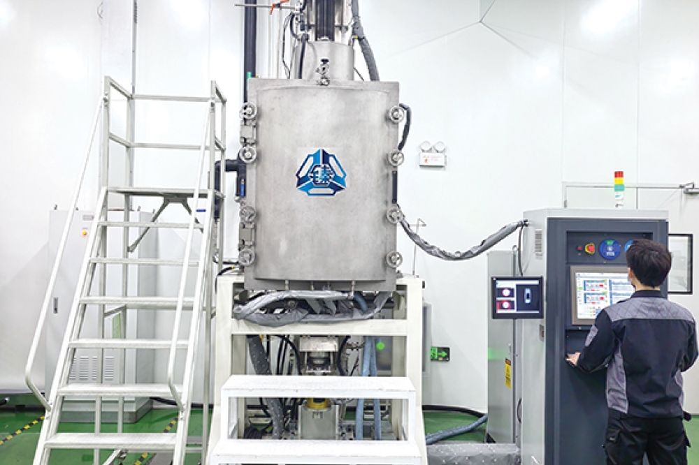
On the manufacturing side, CDimension is already working with Powerchip Semiconductor Manufacturing Corporation (PSMC) to fabricate early circuit-level test structures. By validating its materials through standardised silicon workflows, CDimension aims to reduce integration risk for future commercial products.
CDimension says it is pursuing a dual strategy focused on both materials commercialisation and IC development, with the aim of balancing near-term commercialisation with long-term technology development.
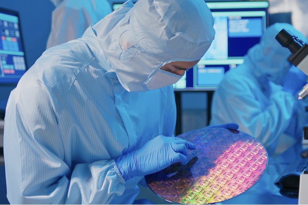
On the materials front, it is providing 2D materials, such as MoS₂ monolayers, to academic and industrial R&D teams working on nanoelectronics, sensors, photonics, and other next-generation systems. This early commercial activity is already generating revenue and building customer relationships.
For IC development, the company is developing proprietary monolithic 3D ICs by integrating 2D materials into foundry-compatible process flows. These architectures are designed to enable future breakthroughs in AI, quantum computing, and high-performance edge systems.
“Our mission is to drive innovation in next-generation semiconductor and integration technologies,” said Jiadi Zhu, CEO of CDimension. “Along the way, we are supplying reliable 2D materials to researchers worldwide, helping them accelerate their work while also expanding the potential markets and applications for these materials. With the support of leading researchers and early foundry partners, we are laying the foundation for the next era of computing hardware.”