
Hot-wall MOCVD helps GaN-on-AlN HEMTs
A collaboration led by Linköping University is raising the bar for the performance of GaN HEMTs grown on AlN substrates. Devices featuring a thin channel and grown by hot-wall MOCVD are claimed to combine a high carrier density with a record mobility for the two-dimensional electron gas (2DEG).
Commenting on this success, Vanya Darakchieva, who is affiliated to both Linköping University and Lund University, remarks: “Achieving this requires growing thin GaN layers on AlN with low impurity and defect densities and excellent structural quality, which is very challenging.”
Key to the team’s success is its MOCVD reactor. “Our Aixtron reactor is unique worldwide, featuring a hot-wall MOCVD process that minimises vertical and lateral temperature gradients while enabling precise control over gas-phase chemistry,” says Darakchieva.
Developing GaN HEMTs on AlN substrates may raise a few eyebrows, given that this foundation has a reputation for its high cost, small size and limited availability. But Darakchieva says that there is the potential to significantly lower costs, thanks to alternative substrate fabrication methods and a growing ecosystem that’s driven by deep-UV LEDs and emerging power and RF applications. She highlights the Swedish deep-tech spin-off Xtal.works, which is developing innovative PVT and CVD growth methods for wide and ultra-wide bandgap semiconductors.
One of the challenges that Darakchieva and her co-workers have faced stems from the 2.4 percent lattice mismatch between AlN and GaN. Once the critical thickness is exceeded when growing GaN on AlN, strain relaxation kicks-in through elastic mechanisms, such as a transition from the two-dimensional to the three-dimensional growth mode, or plastic deformation via dislocation generation.
Efforts are also hampered by the relatively high surface energy of the AlN substrate that leads to a higher gallium adatom binding energy, shorter diffusion lengths, and a tendency for GaN to nucleate as islands.
Despite all these issues, high-quality growth of a GaN epilayer on an AlN substrate is possible by hot-wall MOCVD, which offers stable high-temperature growth conditions.
The Swedish-based team have demonstrated this by using their Aixtron VP508GR reactor to produce a portfolio of GaN-on-AlN heterostructures on small AlN and 4H-SiC substrates.
Following chemical cleaning with a standard process, both substrates were loaded into the hot-wall reactor, annealed and etched under hydrogen at 1340 °C. Formation of the heterostructures began by growing a 300 nm-thick AlN layer at 1250 °C, and then a GaN layer at 1080 °C, using a range of pressures, V-III ratios, and flow rates for the gallium precursor.
Scrutinising samples with scanning electron microscopy revealed that the team’s standard conditions, which provide a smooth surface morphology and excellent electrical properties for a 1 mm-thick GaN layer, lead to incomplete coverage and individual sparse islands when attempting to form a thin channel layer.
Employing a higher flow rate for the gallium precursor enhanced island coalescence and increased layer coverage. Further gains resulted from reducing the growth pressure to 50 mbar – this helped to form fully merged GaN channel layers under optimised conditions.
The team found that despite GaN nucleation on the AlN surface, this foundation led to greater GaN coverage than that realised with a SiC substrate. Darakchieva and co-workers attribute this advantage to the higher out-of-plane thermal conductivity, which led
to higher surface temperatures, and in turn increased adatom mobility and faster clustering and coalescence.
HEMTs have been produced using more promising growth conditions and an AlGaN barrier layer, as well as an AlN interlayer between the GaN channel and barrier layer.
Record mobilities for a GaN channel without an AlGaN buffer of 1910 cm2 V-1 s-1 and 1805 cm2 V-1 s-1 were obtained on SiC and AlN substrates, respectively, using 150 nm-thick GaN channels, produced with a two-step process.
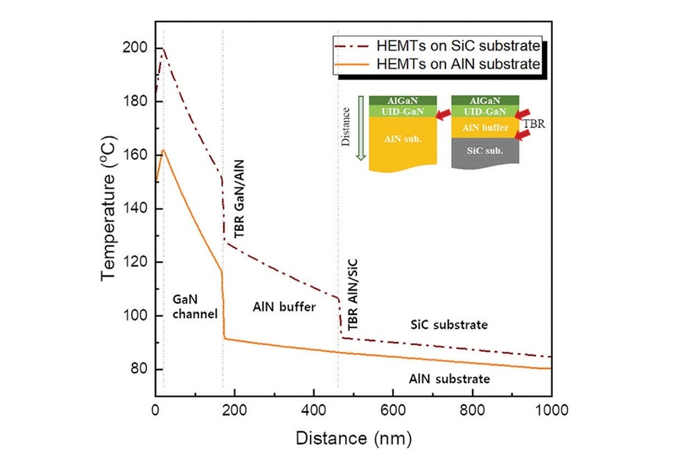
Using measurements of the thermal conductivity of the entire device stack and its individual layers, the team determined the thermal boundary resistance and, through TCAD simulations, estimated the hotspot temperature in the channel.
“Comparing identical device stacks grown simultaneously on AlN and SiC substrates revealed that the device on AlN is approximately 20 percent cooler,” remarks Darakchieva.
Recently, the team have processed devices on SiC and AlN substrates, and they are now evaluating their performance and thermometry.
Reference
M. Kim et al. Appl. Phys. Lett. 127 032104 (2025)
Compared with a SiC substrate, that made from AlN leads to a significant reduction in device temperature.


