

Enkris develops fast, low power microLED product
MicroLED optical devices are emerging as a promising technology for short-distance optical interconnects thanks to their low power consumption and high-density enabling a 'wide-and -slow' architecture side-stepping the increasing power consumption of faster SerDes links .
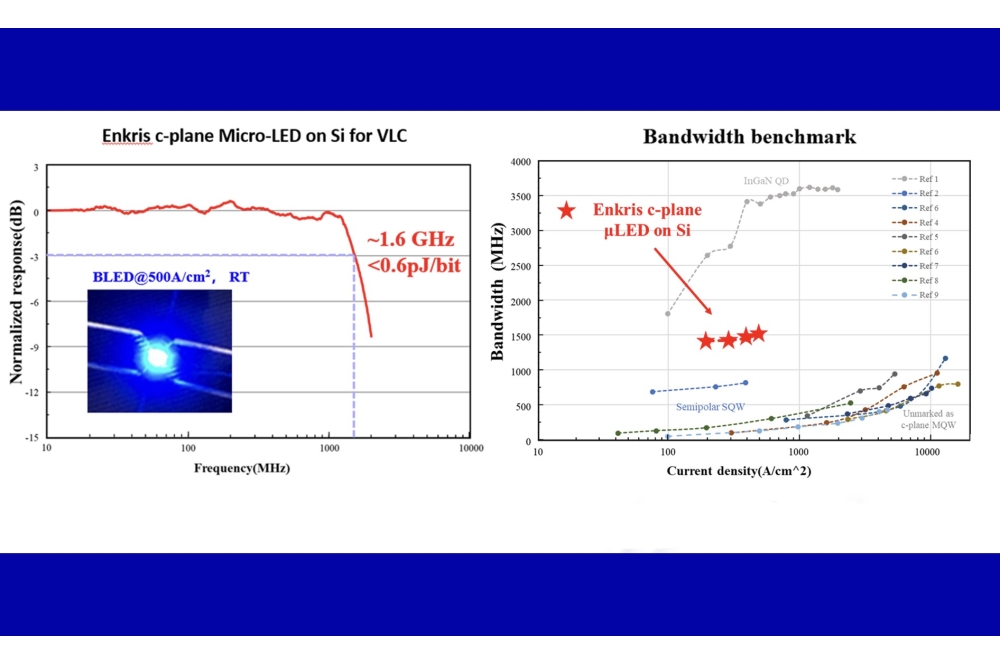
While current microLED optical interconnects primarily rely on sapphire substrates suffering low bandwidth and high driving current density, Chinese firm Enkris Semiconductor has now developed 8inch/12inch GaN-on-Si microLED light source products, achieving a 3dB bandwidth of 1.6 GHz at a current density of 500 A/cm².
It says that the power consumption of the microLED light source can be below 1 pJ/bit.
The results were part of a collaboration between Enkris and Lu Shulong's research group at Suzhou Institute of Nano-Tech and Nano-Bionics, Chinese Academy of Sciences.
To achieve this result, Enkris has optimised the epitaxial structures, material qualities, defects in the active region and device design as well, building on many years experience in GaN epitaxy and a CMOS-compatible microLED process flow. By effectively suppressing the Quantum Confined Stark Effect (QCSE) in the quantum wells, it says, the carrier recombination rate is significantly enhanced.
In addition, the active region area has been reduced to lower device capacitance and minimise RC delay issues.
Enrkis adds that using 8inch/12inch microLED on Si with high bandwidth paves the way for optical device integration on advanced node CMOS by using mature W2W or D2W bonding. Moreover, the technology is compatible with existing hardware architectures and mainstream communication protocols used in high-bandwidth memory, filling the gap in short-range transmission.



