

Scrutinising 50 mm AlN substrates
The recent availability of AlN substrates with diameters of up to 100 mm could be a game-changer for a number of compound semiconductor devices.
This foundation provides a native platform for UVC LEDs and for power electronics based on AlN. The latter has the potential to outperform rivals based on SiC and GaN, thanks to a much wider bandgap and a higher critical electric field. However, the AlN substrate will only provide a bedrock for success on these fronts if it is of sufficient material quality, and can ensure the growth of excellent epilayers.
To investigate if these crucial conditions are met, a US team, led by researchers at the US Naval Research Laboratory (NRL) and including engineers from Crystal IS and Agnitron Technology, has been scrutinising AlN substrates with a diameter of 50 mm, and AlN epilayers grown on this foundation.
Offering a summary of the findings, team spokesman Alan Jacobs from NRL told Compound Semiconductor: “The wafer-scale changes in photoluminescence point toward varying point-defect populations, while the X-ray topography and high-resolution diffraction mapping show there can be off-cut variation or local dislocation density variations, potentially impacting growth, impurity incorporation, and device characteristics.”
The team’s comprehensive study involved Crystal IS AlN substrates with a surface orientation of ± 3°, an absorptivity of less than 30 cm-1 at 265 nm, and a surface bow of less than ± 10 µm.
Atomic force microscope of as-received AlN substrates determined a root-mean-square roughness of about 0.1 nm, and the presence of clear atomic steps, with edges aligned parallel to the flat of the wafer. The team also found a number of depressions, with a depth of around 1 nm, diameters ranging from 100 nm to 400 nm, and curved step edges at the circumference.
After chemical cleaning of the substrates, they were loaded into an MOCVD reactor and annealed at 1250 °C in ammonia to clean and stabilise the surface, prior to the addition of an unintentionally doped, 1 µm-thick layer of AlN at 1250 °C.
Compared to the AlN substrate, its epilayer has a slightly higher macro-roughness, but is free from small depressions. However, there are surface perturbations, with co-located peaks and valleys, having a height deviation of 0.5 nm and a spatial extent of 1.5-2 µm. These features may result from overgrowth of the initially observed depressions.
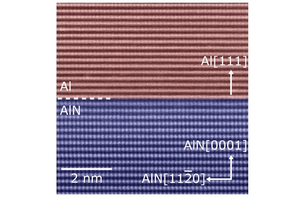
When inspecting AlN material by optical microscopy, the researchers observed bright features, described as spatially inhomogeneous in the radial direction. To uncover their origin, cross-sections were formed with a focused ion beam and imaged with various forms of microscopy. Electron microscopy revealed that these bright features are associated with platelet regions parallel to the wafer surface. The platelets are mainly aluminium, according to energy-dispersive X-ray spectroscopy. This finding is supported by high-angle annular dark-field scanning transmission electron microscopy, which shows that the atomic spacing within the platelet is essentially equal to that for bulk aluminium.
“We were 100 percent surprised by the metallic inclusions,” admits Jacobs, who initially worried about their impact on the performance of power devices, but is now far less concerned, due to their low volume fraction, small size and isolated nature.
“Perhaps there will be some noticeable RF or dynamic switching losses associated with these defects, however, that remains to be seen, and given the sparse nature – and distribution through the full thickness – they may not be near enough devices to have an impact.”
X-ray topography has been employed to determine the dislocation density, which is significantly lower than that of GaN. It’s around 102 cm-2 in the centre of the wafer, and as high as mid-105 cm-2 near the edge.
The team plans to continue to characterise AlN substrates and epilayers, with investigations hopefully extending to 4-inch wafers.
“We are also focusing our efforts toward devices built on these substrates, including AlGaN/AlGaN HEMTs for high power and high temperature operation, vertical device topologies for high voltage and high-power scaling, and potential novel devices enabled by the unique characteristics of AlN,” said Jacobs.
Pictured above; The platelets have an atomic spacing that is essentially equal to that for bulk aluminium, according to high-angle annular dark-field scanning transmission electron microscopy.
Reference
A. G. Jacobs et al. Appl. Phys. Lett. 128 202102 (2026)



