

PVA TePla and Fraunhofer IISB establish AlN lab
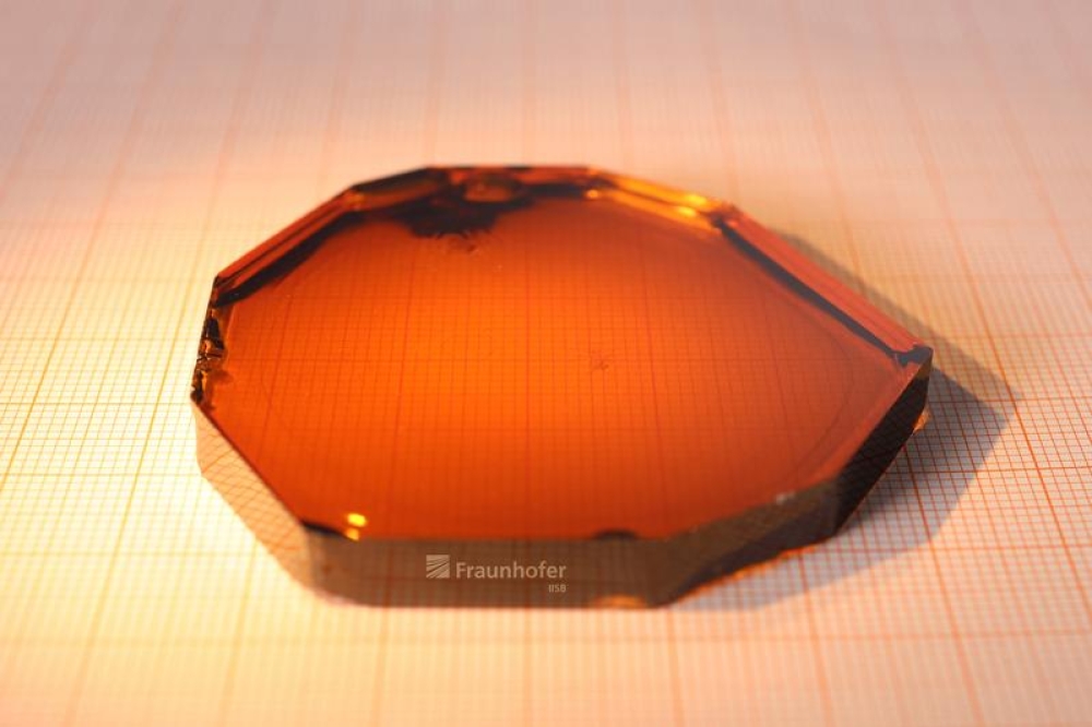
The Fraunhofer Institute for Integrated Systems and Device Technology IISB and PVA TePla AG are pooling their expertise in a joint lab for the production of AlN crystals.
As a European first, this partnership enables industrially supported small-batch production of monocrystalline 2-inch AlN substrates for R&D. This significantly improves the availability of AlN substrates in Europe, which in turn accelerates the development of AlN-based components and systems and their transition to industrial applications.
AlN is one of the most promising materials for the next generation of high-performance electronics. As an ultra-wide bandgap (UWBG) semiconductor, AlN opens up new possibilities in photonics, power electronics, high-frequency electronics, and electronics operating under extreme conditions. To date, the shortage of high-quality, large-area, and cost-effective AlN substrates has been holding back the development of AlN-based electronic systems.
"With the Joint Lab, we are laying the groundwork to ensure a reliable supply of AlN substrates from Europe, thereby opening up new prospects for the next generation of high-performance AlN devices", says Sven Besendörfer, group leader for nitride materials and responsible for AlN material development at Fraunhofer IISB.
"Together with PVA TePla, we are contributing our expertise in industrial crystal growth, thereby creating the prerequisites for the transfer to concrete applications."
In the Joint Lab, Fraunhofer IISB is using its proprietary PVT process technology to produce 2-inch AlN bulk crystals. PVA TePla provides PVT systems for this purpose, which are already in use worldwide for 8-inch-diameter SiC crystals and have now been specially adapted for the growth of 2-inch AlN crystals.
'With AlN, we are actively shaping the next generation of technology following SiC," explains Jan Pfeiffer, VP of R&D at PVA TePla. "Through the Joint Lab, we can directly combine our equipment expertise with the process know-how of Fraunhofer IISB, enabling us to offer market-oriented solutions to our global customers at an early stage. Our shared goal is to stimulate market development in the AlN sector through suitable substrates and to support companies looking to enter this field as technology partners with the right equipment and corresponding process expertise."
The AlN crystals produced in the Joint Lab are further processed at Fraunhofer IISB into epi-ready AlN substrates and, through LZE GmbH, specifically transferred into industrial development and scaling processes.
"For Europe’s semiconductor sovereignty, it is crucial that new key materials are not only developed but also rapidly transferred into industrial applications and scalable value creation. With its market-place for cutting-edge technologies, LZE GmbH provides companies and research institutions with globally unique and open access to AlN substrates. In this way, we help ensure that promising applications for high-volume industrial markets are brought to market more quickly," says Christian Forster, MD of LZE GmbH.
At the same time, Fraunhofer IISB is driving forward the development of 4-inch, and, in the future, 6-inch AlN technology.



