HRL’s GaN: from innovation to qualification

Maintaining the tradition of being ‘first’ in technology innovation, HRL’s latest T3L GaN technology delivers a world-leading high-frequency performance with a process that’s manufacturable, stable, predictable and reliable.
BY SATYAKI GANGULY, F. ERDEM ARKUN, ANDREA ARIAS-PURDUE, DAVE FANNING, ANDY FU, DMITRY VEKSLER, DAN DENNINGHOFF AND ANDREA CORRION FROM HRL LABORATORIES
By offering increases in power, efficiency and bandwidth over other semiconductor technologies, RF GaN devices are continuing to make a substantial impact in commercial and defence applications. But to ensure the future success of this class of device, its progress must not grind to a halt. Due to the proliferation and complexity of RF signals, the electromagnetic environment is increasingly crowded, driving urgent demand for GaN technologies operating at higher frequencies – and in particular, the millimetre-wave range that spans 30 GHz to 300 GHz.
Meeting this need is not trivial. It requires a rethinking of GaN materials and fabrication approaches, including a move away from many of the standard features incorporated into lower-frequency technologies, such as standard annealed ohmic contacts, large field-plates to manage electric fields, and the standard AlGaN/GaN HEMT epitaxial structure.
Unfortunately, those that take on the challenge of moving to higher frequencies also come up against a number of trade-offs. To give just one example, when decreasing the gate length to sub-100-nm dimensions and eliminating field plates to enable high-frequency operation, peak electric fields in the device increase, impeding reliability. What’s needed are out-of-the box, innovative solutions.

Figure 1: The evolution of HRL’s millimeter-wave GaN foundry offerings over time.
At HRL Laboratories, LLC, we have a long history of exceling on this front. By redefining the boundaries of what’s possible today, we invent solutions to tomorrow’s problems. Employing an ownership model that prioritises purpose over profit, we invest in ambitious ideas and take strategic risks on projects that significantly advance the state of the art, pursuing paths that others might overlook. This culture is reflected in our legacy of groundbreaking work on high-frequency GaN.
For many years, our portfolio of millimetre-wave GaN devices and circuits has featured cutting-edge innovations that break performance trade-offs and push the boundaries for high-frequency GaN. One of our latest technology nodes – T3L GaN – builds upon our previous successes, while adding innovations that ensure high linearity and reliability, such as a graded epitaxial structure and a gate mini-field-plate. In recent times, we have also invested tremendous effort into GaN technology maturation, qualification, model development, and external foundry services. The result is that today we are offering GaN with world-leading high-frequency performance – such as T3L – to external designers via reliable, mature, open foundry offerings.
HRL GaN odyssey
We have been investing in GaN materials, transistors, and circuit development since the late 1990s, and we have a long history of ‘firsts’ for RF GaN MMICs, particularly in high-frequency technology demonstrations.
Our early investments associated with in-house epitaxial growth capability enabled innovations such as n+ GaN ohmic contact regrowth by MBE, and vertically scaled layer structures necessary for high-frequency performance.
As we continue to develop and advance our GaN technology, we draw on our extensive expertise in high-frequency MMIC design and fabrication. Our background includes a strong track record as a provider of high-frequency GaAs and InP-based circuits.
Key milestones in GaN RF technology include unveiling the first Ka-band GaN MMIC power amplifier at the 2004 IEEE International Microwave Symposium, the first W-band GaN MMIC power amplifier at the 2006 International Electron Devices Meeting, and the first G-band GaN MMIC at the 2014 IEEE Symposium on Compound Semiconductor Integrated Circuits.

Figure 2. For Ka-band amplifiers linearity versus DC power consumption with typical linearity FOM of around 0 dB has been shown. Star represents the fiducial point illustrating HRL’s T3L GaN linearity that sets HRL apart. Adapted from J. -S. Moon et al. International Microwave Symposium - IMS 2022, pp. 302-304, 2022.
Over the years, our high-frequency GaN technology nodes – which have utilised ‘T’-gates, as opposed to gamma- or field-plate gates – have targeted progressively higher-frequency operation (see Figure 1). Our T3L node is built upon our 40 nm-gate T3 node, but features key modifications to improve linearity and dynamic range – this results in an enviable combination of outstanding linearity, noise, output power, and efficiency for millimetre-wave applications. Much of this pioneering work in high-frequency GaN was made possible through financial support from the US government, with programmes such as DARPA WBGS, DARPA NEXT, and DARPA DREAM, among others.
HRL T3L GaN technology
Our T3L GaN HEMT technology was initially developed under DARPA’s Dynamic Range-enhanced Electronics and Materials (DREaM) programme, which had the goal of developing new designs and materials for RF transistors with an unprecedented dynamic range in millimetre-wave systems. To succeed in this endeavour, we combined a graded-channel AlGaN/GaN epitaxial structure, providing precise control of transistor transconductance, with a scaled 40-nm T-gate and mini-field-plate. One of the key merits of the graded-channel epi and mini-field-plate is a distribution of the electric field across the device’s active area that improves linearity and reduces signal distortion – that’s particularly beneficial for high-frequency applications, where RF signal integrity and linearity are crucial. Meanwhile, the short gate length supports a high cut-off frequency (fT) of 170 GHz, and a maximum oscillation frequency (fMAX) of 347 GHz.
Drawing on these strengths, our GaN MMICs that incorporate the T3L transistor technology and on-chip pre-matching networks have demonstrated a world-record peak power-added efficiency of 45 percent at 94 GHz, and a corresponding power density of more than 2 W mm-1. These two characteristics are key performance metrics for efficient power amplifiers. The power-added efficiency of our GaN MMICs at 30 GHz is world-beating, with values as high as 70 percent.
Modern-day phased arrays and high-dynamic-range RF front ends require amplifiers with high linearity. Traditionally, this linearity requirement has been fulfilled with low-noise amplifiers, operating with a higher DC power consumption, or power amplifiers that are run at a reduced power-added efficiency and power density.

Figure 3. Three-temperature accelerated life (3T-ALT), high-temperature reverse-bias (HTRB), and RF high-temperature operating life (RF-HTOL) tests of HRL’s T3L GaN. (a) Median-time-to-failure (MTTF) versus junction temperature for T3L GaN discrete devices under DC-ALT stress. Red data points represent the extracted MTTF values at the stress temperatures, while the green solid line is the fit and extrapolation as described in the text. The star represents the fiducial point to illustrate the predicted MTTF lifetime at the junction temperature, Tj, of 150 °C, of more than 1 x 10⁷ hours. (b) Threshold voltage of discrete devices during HTRB stress and (c) RF output power (Pout) during HTOL stress, both showing excellent stability up to at least 1000 hours.
Neither of these options is preferable. Industry is reluctant to meet linearity requirements by taking a hit in efficiency or consuming more power, especially as payload power needs to be allocated to increased bandwidth and newer software-defined features. Moreover, many airborne platforms are size, weight and power (SWaP) constrained.
What’s urgently needed are devices with a high linearity-to-power-consumption figure-of-merit. In this regard, a common figure-of-merit for benchmarking is the ratio of the Output Third-Order Intercept Point (OIP3) (a measure of linearity) to DC power consumption. Judged against this metric, known for short as OIP3/PDC, our T3L GaN technology that employs key design and process breakthroughs delivers a record 17.5 dB at 30 GHz. That’s a jaw-dropping improvement, more than 30 times better than the best previous Ka-band low-noise amplifiers featuring GaAs pHEMTs and AlGaN/GaN HEMTs (see Figure 2).
Key features of our T3L GaN technology include two-level metal interconnects with 5 µm plated airbridges, 50 Ω/sq. thin-film resistors, 300 fF mm-2 metal insulator metal capacitors, and 50 mm SiC with through-substrate vias and backside metal.
Our T3L GaN is well-positioned for success in a range of cutting-edge applications within the millimetre-wave domain. Deploying our technology in 5G and beyond wireless communication enables faster data transmission and improved signal quality; in high-resolution radar systems, T3L GaN provides better target detection and imaging capabilities; in electronic warfare and defence systems, T3L GaN enables robust performance in challenging environments; and last but not least, in satellite communications T3L GaN ensures reliable, efficient signal transmission over long distances.
T3L GaN technology qualification
Recently, we have invested heavily in the qualification and maturation of our RF GaN technology, to meet the ever-growing demand and requirements of key strategic customers. Lifetime assessment is the first step towards meeting such expectations.
The first inception of our T3L GaN on the DARPA DREaM programme demonstrated the tremendous potential of our technology. Since then, by devoting much effort to technology maturation and qualification, we have been led to implement several minor proprietary changes to the epitaxial structure and fabrication processes, to further improve yield, manufacturability, and reliability.
To understand the lifetime of our first-in-class sub-100-nm GaN HEMTs, we have undertaken temperature-accelerated lifetime testing on our 4 x 37.5 µm T3L GaN discrete transistors with a dissipated power of around 4 W mm-1 and junction temperatures ranging from 300 °C to 380 °C (results are shown in Figure 3). Note that, to drive devices to failure, we have intentionally employed stress temperatures that are far higher than the recommended operating condition, which typically ranges from 150 °C to 225 °C.
For this study, we defined the failure criteria as a 20 percent degradation in device on-resistancefrom its initial value. To determine values for the median-time-to-fail (MTTF) and lifetime, we analysed the failure time distribution with an Arrhenius temperature-accelerated lifetime model, lognormal statistics, and maximum likelihood estimation.
Based on this approach, we find that despite having one of the shortest gate lengths in the GaN industry, our T3L device lifetime is no shorter than 100 years at a junction temperature of 150 °C. This is a MTTF benchmark that other GaN manufacturers typically strive for.
In addition to temperature-accelerated life testing, we have also performed off-state high temperature reverse-bias (HTRB) and on-state RF high temperature operating life (RF-HTOL) reliability testing on T3L devices (see Figure 3). For HTRB testing at an ambient temperature of 150 °C, we stressed a group of discrete transistors from multiple wafers using a gate bias of -7 V and a drain bias of 35 V, which corresponds to 250 percent of the operating quiescent voltage (14 V). Under these conditions, we evaluated the stability of various device parameters, such as the threshold voltage.
Applying these conditions for HTRB testing, we determined that device performance is stable up to at least 1000 hours. This is a key reliability benchmark.
On-state qualification of our T3L MMICs through RF-HTOL stress also showed excellent stability, with minimal shift in critical RF-paraments after 1000 hours of stressing.
Successfully passing 1,000 hours of HTRB and RF-HTOL testing, in addition to hitting the state-of-the-art MTTF benchmark, serves as a testament to our stable, predictable, and reliable GaN T3L process.
Note that our GaN manufacturing process aligns with a remark made by one of the fathers of statistical process control, the US engineer Harold Dodge, who is famous for the phrase ‘you cannot inspect quality into a product’. The implication of his statement is that it’s critical to build quality and reliability into the product during the manufacturing process. Abiding by this philosophy, we do not implement any additional burn-in or screening when choosing devices for reliability testing. Instead, all our reliability results come from devices randomly picked across multiple wafers after fabrication.
According to a T3L GaN wafer map of peak fT and gate leakage current, tested on in-line process control monitors, there is excellent uniformity associated with our T3L GaN process fabricated on a 100 mm SiC wafer (see Figure 4, which has an inset that shows a schematic cross-section of a W-band capable T3L GaN transistor, as well as a corresponding scanning electron microscopy image).

Figure 4. Wafer map of a typical T3L GaN (gate length less than 100 nm, source-to drain of 900 nm) showing uniform peak fT at a VDS of 5 V and gate leakage current density measured at VDS = 8 V and VGS = -5 V. Schematic cross section and the corresponding scanning electron microscopy image of a representative T3L GaN transistor taken from such a wafer is shown in the inset.
Technology maturation and foundry service
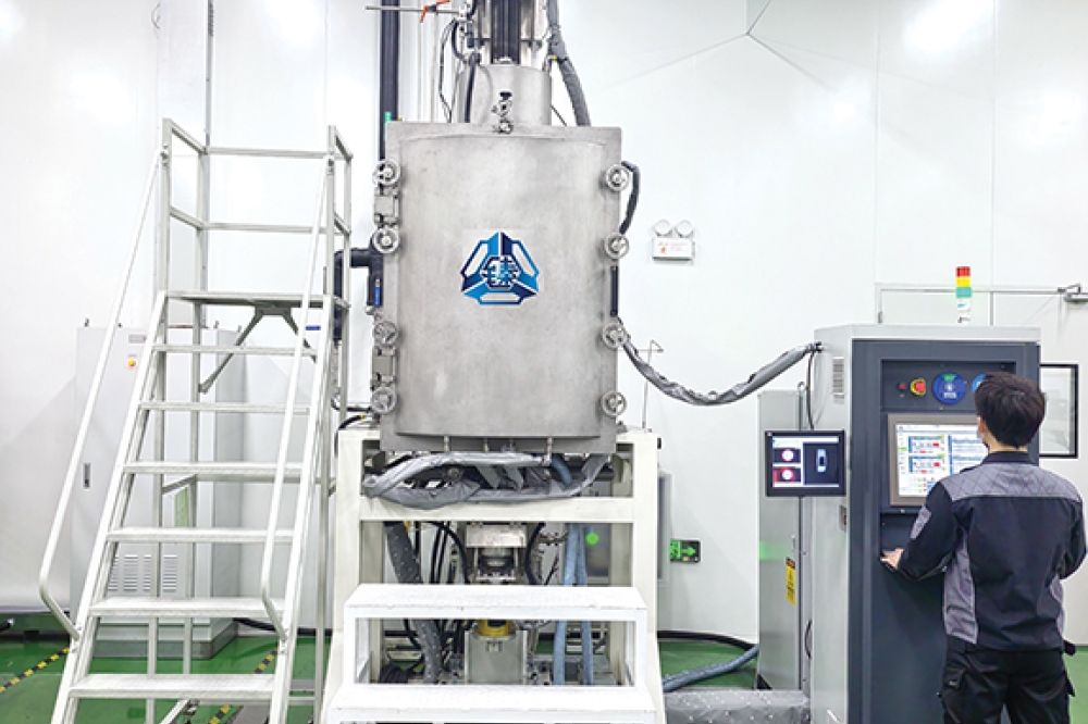
We are the first fab (ISO 9001 certified) to develop and offer a sub-100 nm GaN MMIC process technology through our foundry services. With US government support, in 2019 we launched an open commercial multi-project-wafer (MPW) foundry service for our 40 nm GaN-on-SiC T3 technology, and since 2021 we have offered quarterly MPW runs. To-date, we have sold 86 MPW tiles to 30 unique customers. Our foundry services include process design kits (PDKs) in both ADS and AWR, secure management of customers’ design verification, wafer microfabrication, RF probing, and the delivery of singulated MMICs.
To continue to advance our T3L technology node, this year we are launching a T3L GaN MPW service, and adding advanced interconnect features, such as copper pillars for flip-chip compatibility.
Historically, our GaN foundry interests have been balanced across research institutions, companies in the aerospace and defence sector, and commercial private-sector entities. Thanks to the maturation of our sub-100 nm GaN processes, we have seen increasing demand, especially for applications in the V/W-bands. Customers are encouraged to engage with our open foundry for GaN PDK and device model access and support for low-to-moderate volume production.
Beyond T3L GaN
In addition to our T3L RF-GaN technologies, we continue to innovate, motivated by the goal of pushing the boundaries of future technologies that will be transformative for the warfighter. One such innovation is N-Polar GaN, a technology we are exploring for its potential to deliver higher power. N-Polar GaN is showing promising capabilities compared with traditional GaN, but it is still advancing through the maturity stages, supported by early government investments in both academia and industry.
We are also making strides in the Ultra-Wide Bandgap Semiconductors (UWBGS) programme that’s funded by DARPA. This initiative focuses on developing key processes for realising next-generation devices, including high-efficiency UVC LEDs, laser diodes, high-power RF transistors, and power-conversion electronics.
Through these efforts, we continue to position ourselves at the forefront of technological advancements that will shape the future of military and commercial applications.
By combining world-record efficiency, output power, linearity, and noise figures with excellent device reliability, stability, and uniformity, our current GaN technology is uniquely positioned to address rapidly evolving needs in the millimetre-wave RF application space. On top of that, our heavy investment in maturation and capacity to support customer engagements is ensuring a bright future for our GaN, and helping to continueto shape the future of GaN for the broader community.
HRL Laboratories conducts contract research and development with support from various US government agencies, including DARPA, US Air Force, OUSD, and ONR. The organisation gratefully acknowledges this vital support in driving the advancement of cutting-edge technologies and scientific innovation.