Stacked OLEDs make ultra bright microdisplays
Researchers at the Fraunhofer Institute for Photonic Microsystems IPMS have developed novel OLED stacks that enable exceptionally bright microdisplays. These will be presented for the first time at SPIE AR VR MR 2025, from January 28 to 29, 2025, in San Francisco.
Users of augmented reality (AR) glasses require especially bright displays in daylight to clearly recognise content. High brightness and low power consumption are therefore crucial development goals, as optical systems — such as AR glasses — exhibit high brightness losses and wearable devices are limited by battery storage. The Fraunhofer IPMS is now introducing a highly efficient, monochrome OLED microdisplay with a brightness of over 70,000 Nits. The OLED stack used even achieves over 200,000 Nits on reference substrates.
Johannes Zeltner, a PhD student at Fraunhofer IPMS, explains: “By stacking OLED layers, this outstanding brightness was achieved. The individual OLED units are ‘series connected’, which increases the brightness with each additional unit without raising the current density in the component. This can be utilised to either achieve extremely high brightness or, at a given brightness, to significantly reduce the current density that determines lifetime. Measurements have shown that when comparing a 1-unit and a 2-unit OLED, the lifetime LT95, i.e., the drop in brightness by 5 percent, at 50,000 Nits can be significantly improved from 900 to 1300 hours.”
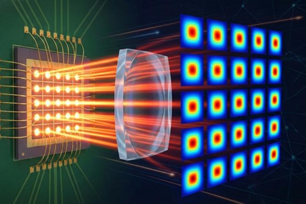
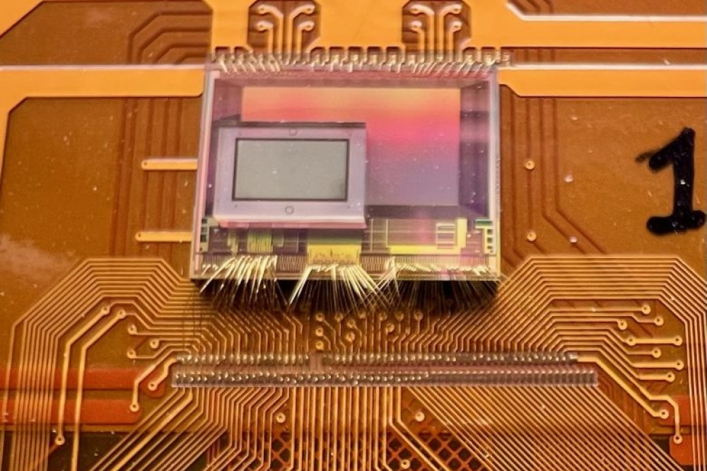
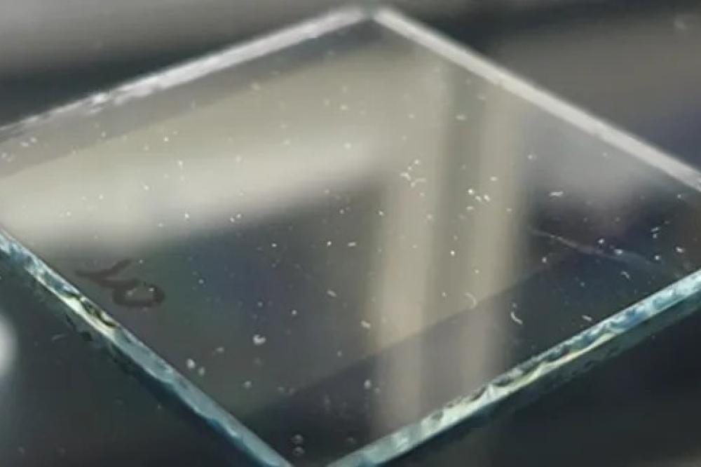
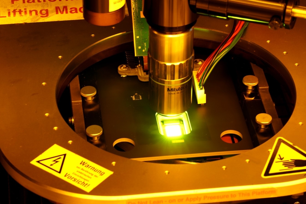
The current efficiency and brightness of 1-, 2-, and 3-fold stacked OLEDs were initially evaluated on passive test substrates and were subsequently successfully transferred to 0.62-inch CMOS backplanes with SXGA resolution. New challenges for further research have emerged: While conventional OLED displays often have several tens of micrometers between subpixels, in microdisplays, it is only a few hundred nanometers. This can lead to crosstalk between adjacent pixels in thicker layer stacks and multiple stacked OLEDs in microdisplays. Approaches to reduce this crosstalk are in preparation. Furthermore, the work has shown that multiple stacking allows for narrowband emission with high brightness. The spectral emission can be specifically adjusted, enabling the use of optical concepts with special requirements, such as waveguides or holographic elements.
The researchers are convinced that the ongoing development towards ever higher brightness and improved lifetimes of OLED technology secures a firm place in the field of AR applications. Nevertheless, there is a continuous need for research, e.g., on optical crosstalk, improved OLED materials, and novel backplane architectures.