Bristol University team makes GaN breakthrough
Research led by University of Bristol could supercharge 6G delivery by making GaN-based RF power amplifiers quicker, more powerful and more reliable.
The breakthrough, published in the journal Nature Electronics, uses a latch-effect in multichannel GaN transistors to unlock greater RF device performance.
According to co-lead author Martin Kuball, professor of physics at the University of Bristol, the new GaN-based architecture would make it easier to communicate and transfer vast volumes of data, driving forward 6G developments in areas such as remote diagnostics and surgery, advanced driver assistance systems, virtual classrooms and more.
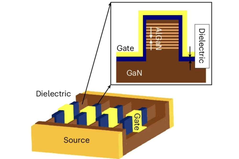
At the latching condition, drain current sharply transits from an off-state value to a high on-state value with a slope less than 60 mV per decade. The latching condition is reversible and non-degrading, and the researchers have shown that it can lead to improvement in the transconductance characteristics of transistors, implying improved linearity and power in RF power amplifiers. The devices have parallel channels which use sub-100nm side fins to control the flow of current passing through the devices.
Co-lead author Akhil Shaji, honorary research associate at the University of Bristol, explained: “We have piloted a device technology, working with collaborators, called superlattice castellated field effect transistors (SLCFETs), in which more than 1000 fins with sub-100 nm width help drive the current. Although SLCFETs have demonstrated the highest performance in the W-band frequency range, equating to 75 gigahertz -110 GHz, the physics behind it was unknown.
“We recognised it was a latch-effect in GaN, which enables the high radio frequency performance.”
The researchers then needed to pinpoint exactly where this effect occurred, by simultaneously using ultra precision electrical measurements and optical microscopy, so it could be further studied and understood. After analysing more than 1,000 fins findings located this effect to the widest fin.
Kuball added: “We also developed a 3D model using a simulator to further verify our observations. The next challenge was to study the reliability aspects of latch effect for practical applications. The rigorous testing of the device over a long duration of time showed it has no detrimental effect on device reliability or performance.
“We found a key aspect driving this reliability was a thin layer of dielectric coating around each of the fins. But the main takeaway was clear – the latch effect can be exploited for countless practical applications, which could help transform people’s lives in many different ways in years to come.”
Next steps for the work include further increasing the power density the devices can deliver, so they can offer even higher performance and serve wider audiences. Industry partners will also be bringing such next generation devices to a commercial market.
Pictured above are schematics of a portion of a SLCFET having multiple (1,000s) of fins along with the cross-section of a single fin with its multiple conducting channels.
Reference
Kumar, A.S., Dalcanale, S., Uren, M.J. et al. Gallium nitride multichannel devices with latch-induced sub-60-mV-per-decade subthreshold slopes for radiofrequency applications. Nat Electron (2025).