
Tiny pyramids boost perovskite/silicon tandem efficiency to 30%
Combining crystalline silicon with wide-bandgap perovskite can increase solar cell conversion efficiencies. But mechanical stresses between the silicon bottom cell and the perovskite top cell, often lead to delamination and device degradation.
Now, a team from the Shanghai Institute of Microsystem and Information Technology (SIMIT) of the Chinese Academy of Sciences, alongside collaborators from the University of Chinese Academy of Sciences and Southwest Petroleum University, has developed a potential solution to this structural challenge.
In their study 'Enhanced performance and flexibility of perovskite/silicon tandem solar cells via uniform submicron pyramids' published in Engineering Energy, the researchers demonstrate that reducing both the thickness of the silicon wafer and the size of surface texturing pyramids improves the wafer's flexural strength.
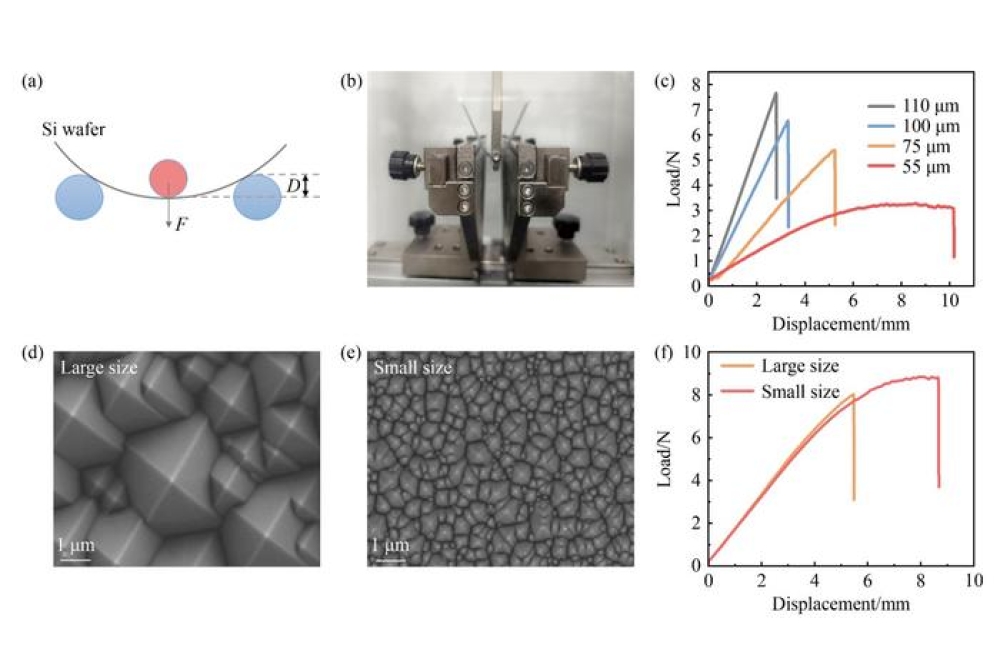
Standard V-shaped valleys between large silicon pyramids act as stress concentration points, making thin wafers prone to cracking under bending. By minimising these pyramid structures, the stress concentration is alleviated, enhancing the material's mechanical flexibility.
To achieve this, the team used precisely controlled wet-etching process to fabricate small-sized, high-density, and highly uniform submicron pyramids on 55 µm silicon wafers. They identified that an optimal etching duration of 360 seconds produced a dense array of uniformly sized pyramids (ranging from 800 nm to 1.7 µm) that balanced optical light-trapping capabilities with mechanical stability.
This submicron texture improved the minority-carrier lifetime and achieved an excellent implied open-circuit voltage. In addition, the homogeneous submicron structure facilitated complete infiltration of the perovskite layer, promoting uniform nucleation and isotropic grain growth. And the improved structural quality suppressed non-radiative recombination losses and improved interfacial contact properties, according to the paper.
The team built monolithic flexible perovskite/silicon tandem solar cells as a proof of concept and achieved a steady-state power conversion efficiency (PCE) of 30.04 percent. The optimised devices demonstrated stable power output and negligible hysteresis.
The researchers believe this approach provides an effective surface engineering strategy to resolve the conflict between optical performance and mechanical stability in thin silicon wafers, with potential for future of low-cost, lightweight, and flexible PV applications, including aerospace technology, building-integrated photovoltaics, and wearable electronic devices.
Pictured above: (a) The principle of the three-point bending test; (b) experimental setup for test; (c) load-displacement responses of silicon wafers with different thicknesses; (d) SEM image of silicon surface with large-sized pyramids;(e) SEM image of silicon surface with small-sized pyramids; (f) load-displacement responses of silicon wafers with different pyramid sizes.


