
IVWorks reGaN tech enables World's first 742GHz GaN HEMT
A GaN HEMT incorporating the Korean company IVWorks' proprietary reGaN selective regrowth technology has become the world's first GaN transistor to achieve a maximum frequency (fmax) exceeding 700 GHz.
This achievement was demonstrated through a 45nm GaN HEMT device developed by Daehyun Kim's research team in the school of electronics engineering at Kyungpook National University in Korea. It was unveiled on June 18 at the VLSI Symposium 2026.
The research team fabricated a GaN transistor with a 45 nm gate length and achieved a record-breaking fmax of 742 GHz, establishing a new benchmark for RF performance in GaN transistor technology. The device also achieved a record average frequency metric (favg) of 497 GHz, the highest value reported to date for any GaN transistor technology.
These results demonstrate that GaN semiconductors possess sufficient performance competitiveness even in the ultra-high-frequency regime and can serve as a viable platform for future sub-terahertz and terahertz electronic systems.
While InP-based transistors have long dominated the sub-terahertz frequency regime due to their exceptional electron transport properties, their relatively low breakdown voltage limits output power and system scalability.
In contrast, GaN semiconductors offer a unique combination of high breakdown electric field, high power density, and excellent thermal robustness, making them attractive candidates for next-generation high-frequency and high-power applications. However, achieving ultra-high-frequency performance with GaN has remained a significant challenge. To overcome these limitations, the research team employed an advanced 45 nm gate process and optimised device architecture to maximise high-frequency performance.
A key enabler of this achievement was IVWorks' proprietary reGaN selective regrowth technology. Developed exclusively by IVWorks, reGaN selectively regrows heavily doped n-type GaN in the source and drain regions, significantly reducing contact resistance.
As a co-research partner in this study, IVWorks demonstrated excellent process uniformity across the entire 4-inch wafer and achieved outstanding reproducibility. Furthermore, the company reduced regrowth interface resistance (Rint) to 0.027 Ω·mm, approaching the theoretical limit achievable at the corresponding carrier concentration.
Daehyun Kim of Kyungpook National University commented: “This research pushes the RF performance limits of GaN HEMTs to a new level and demonstrates the potential of GaN semiconductors for ultra-high-frequency applications through the world's first demonstration of a GaN HEMT with an fmax exceeding 700 GHz. The study is particularly meaningful as a successful example of industry–academia collaboration, combining advanced epitaxial growth and regrowth technologies from industry with the university’s expertise in device and circuit research.”
He added: “Building on this achievement, we plan to further accelerate the development of next-generation GaN electronic devices targeting terahertz-frequency applications for 6G communications and advanced defense technologies.”
The achievement further highlights the growing potential of GaN technology to expand beyond traditional RF and power electronics into emerging sub-terahertz and terahertz applications, including 6G communications, advanced radar systems, satellite communications, and next-generation defense electronics.
Young-kyun Noh, CEO of IVWorks, said: “reGaN is a core technology that has already passed quality qualification at a major foundry and has been adopted for volume production. This achievement demonstrates that our Hybrid-MBE-based reGaN platform is not only manufacturing-ready, but also a key enabling technology for next-generation sub- terahertz and terahertz GaN electronics. We are proud to see IVWorks technology contribute to a world-leading research milestone.”
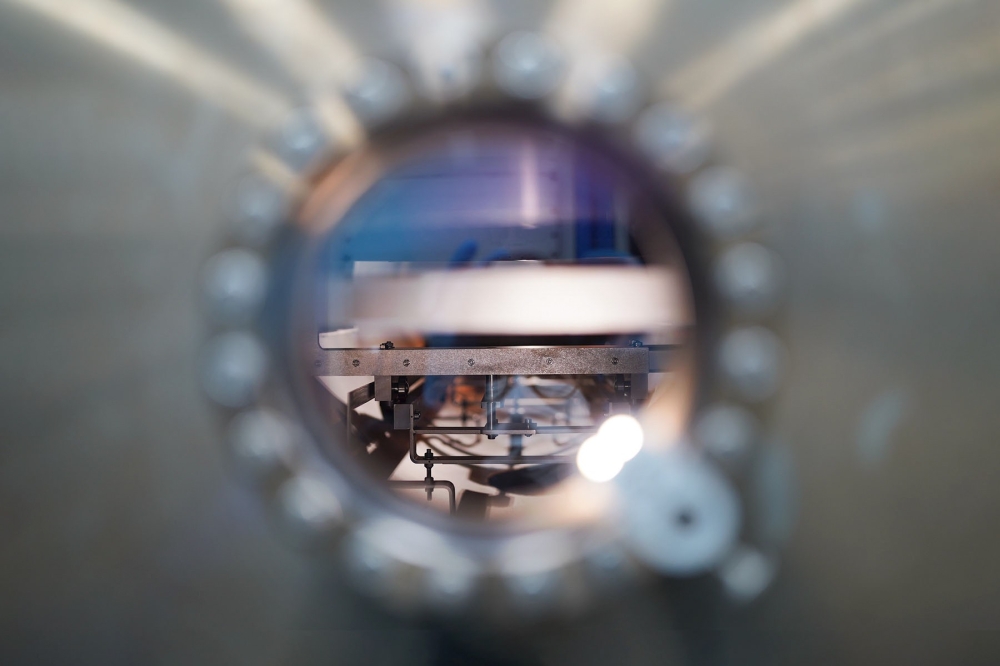
Pictured above: Interior view of IVWorks' Hybrid MBE system used for the proprietary reGaN selective regrowth process. The low-temperature, ultra-high-vacuum growth environment minimises device degradation during regrowth and enables ultra-low-resistance n+GaN source/drain formation for advanced GaN HEMTs.


