The golden age of silicon carbide: 25 years of innovation

During the last 25 years, Cree has had numerous successes, including increasing the size of its SiC substrates, eradicating micropipes and bringing to market SiC diodes, SiC MOSFETs and GaN HEMTs
BY JOHN PALMOUR AND JOHN EDMOND, CO-FOUNDERS OF CREE
The history of SiC begins a very long time ago. It is found in the collisions of meteors, which hit our planet to create the only naturally occurring SiC, located in places that include Canyon Diablo in Arizona. Fast-forward to the twentieth century and we had developed the expertise to synthesize this wide bandgap semiconductor material. However, it is only over the course of the last 25 years that SiC has become an integral part of our lives, featuring in cars, cell phones, radar technology and an array of other applications.
It is fascinating to follow the story of how a material made from meteors’ impacts is now in the palm of our hands. SiC first came into the spotlight in 1907 when it created, by accident, the first LEDs, in the hands of Captain Henry Joseph Round. When this radio pioneer, who moved from the UK to New York to work for the Marconi Company, passed a current through SiC, to his great surprise he witnessed light emission. As well as being deployed in early radios, this material initially found use in abrasives. Throughout the early and middle part of the twentieth century, slow progress occurred, but from then on SiC has undergone a rapid acceleration.
Driving much of this change has been Cree, the company we co-founded in 1987. Formed by a team of researchers previously employed at North Carolina State University, when we embarked on this venture we still had much to learn about the potential of SiC. Back then we knew how much promise this material held as a semiconductor and LED in commercial applications, but we did not know how to get there, and methods were still to be established for efficiently producing the SiC crystals, a pre-requisite to high-volume device production.
During those early years we were buoyed by several crucial breakthroughs. Our milestones included the first commercially available blue LED, and the development of the first commercial SiC wafers. Although our substrates were only 1 inch in diameter and quite expensive, we could grow a business from them.
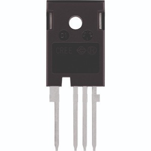
A Wolfspeed 650 V MOSFET.
These successes have provided the bedrock for much more progress over the past 25 years. During this time, SiC has gained commercial momentum that continues to accelerate to this day. We are now in the midst of one of the largest potential transformations in the entire semiconductor industry since the shift in silicon technology from bipolar to CMOS in the 1980s.
Mainstream breakthrough
One of our big, early successes came in 1996, when our blue LEDs were designed into the dashboard of Volkswagen vehicles. Prior to that, we had been selling less-efficient SiC LEDs, but in 1995 we introduced successors based on GaN-on-SiC. Our win with Volkswagen provided the first large-scale use of GaN-on-SiC LEDs in vehicles and signalled an acceptance of this technology – it had matured to a point where it could be adopted by a mainstream automotive player. Key to this acceptance, starting back then and maintained today, is the supply of SiC material. In the early 1990s it was extremely difficult to efficiently and effectively grow SiC crystals, which provide the foundation for LEDs and other devices.
Part of the reason why it is so challenging to produce high-quality SiC substrates is that there are more than 200 different crystal structures associated with various polytypes, and only a few are suitable for the semiconductor market. Adding to the complications, crystal growth requires temperatures nearing 2,500 °C. It’s hard to have a feel for such a high temperature, but to put it in perspective, it is half the temperature of the sun and significantly beyond that of molten lava, which is in the range of 1,700 °C.
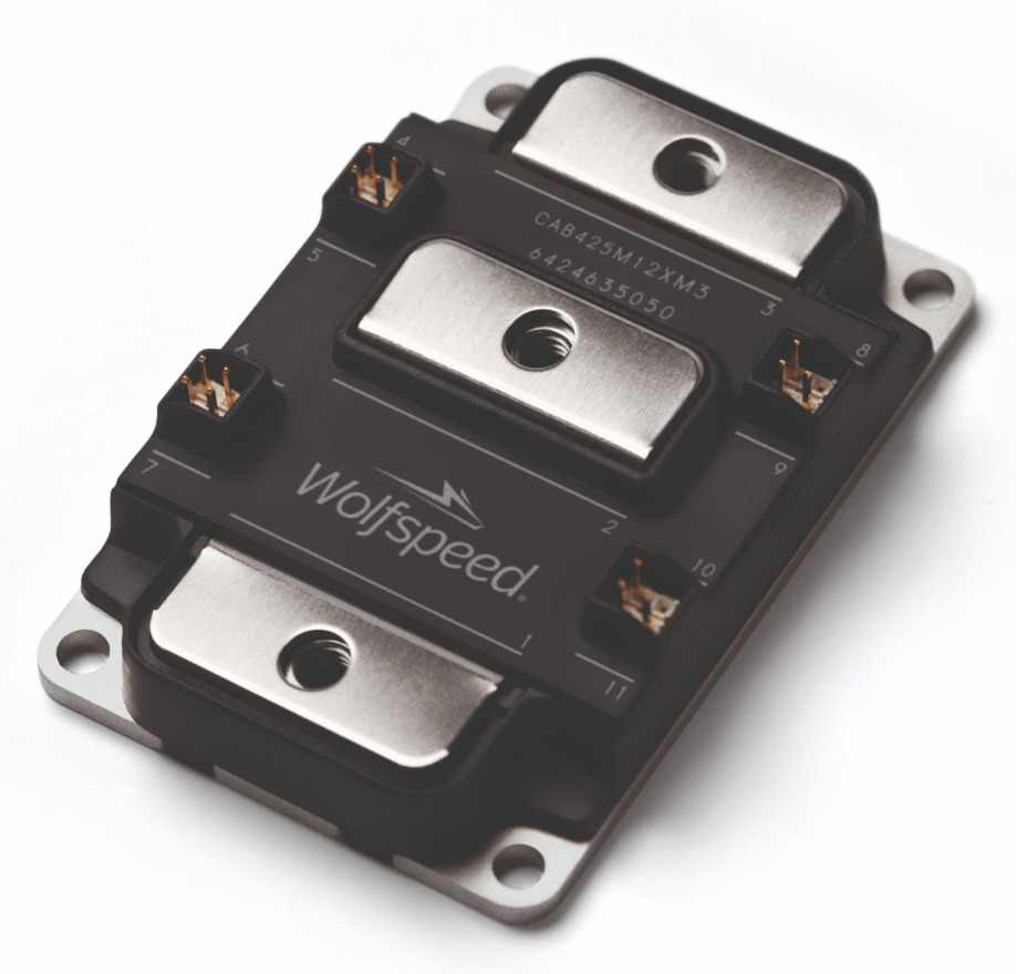
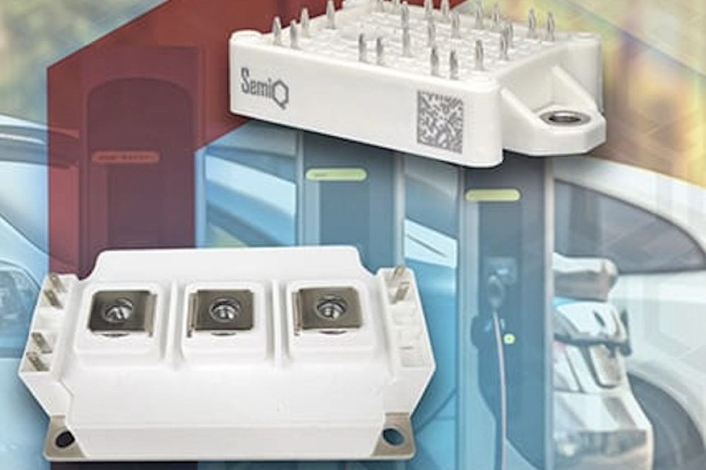
Wolfspeed’s XM3 style SiC Power Module.
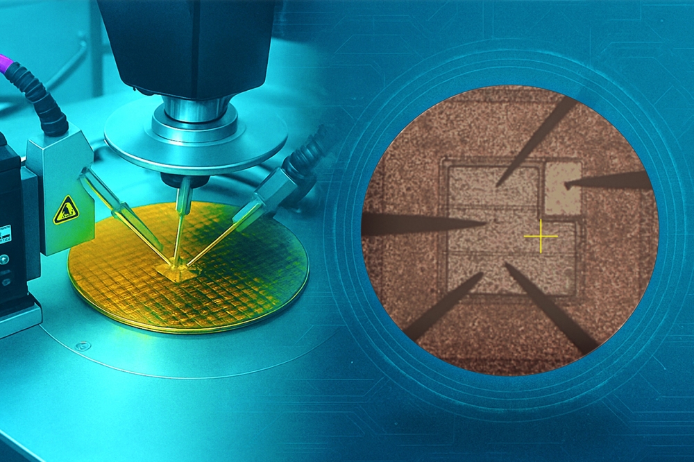
Over the years, our engineers have developed and refined processes that have enabled us to produce single-crystal boules. By increasing the size of these boules, which have limited crystal defects, we have progressed from 2 inch wafers to those that are 3 inch, 4 inch, 6 inch and now 200 mm. This advance stems from having far more development cycles than any other SiC producer. Today we make more than 60 percent of all SiC material. But more importantly, by virtue of the large number of wafers we have made in support of the LED business since 1989, we have produced more than 96 percent of all SiC wafers used in the last 25 years.Sustaining the needs of a major auto manufacturer drove our first breakthrough in our production of SiC. And this is still a topic of conversation in today’s market, where makers of automobiles are integrating SiC in far higher volumes into the drivetrain and chargers of mass-market, battery electric vehicles.
A lighting revolution
Following that first large-scale automotive use of LEDs, the world experienced a meteoric rise in cell phones. Previously a luxurious, somewhat novelty item for the well-to-do, it quickly became a must-have device for many. Since then, handset makers have been churning out millions of units every year.
When the market ramped in 2001, manufacturers of mobile devices started to incorporate LEDs into their latest models. Initially they backlit keypads, and a few years on, they were the light source for colour screens. They are ideal for that task, due to their low energy consumption, small footprint, robustness, and capability to be driven by a battery. The substantial volume of LEDs produced for this market spawned another huge leap forward for GaN-on-SiC sales.
GaN-based LEDs had now found their first killer application. However, although they had made much progress, they still had a long way to go before they could be viewed as a viable candidate for everyday lighting. Before that could happen, there needed to be an expansion in the colour palette generated by these sources, a hike in their efficiency, and a drop in price so they could be a competitive rival to the incandescent bulb.
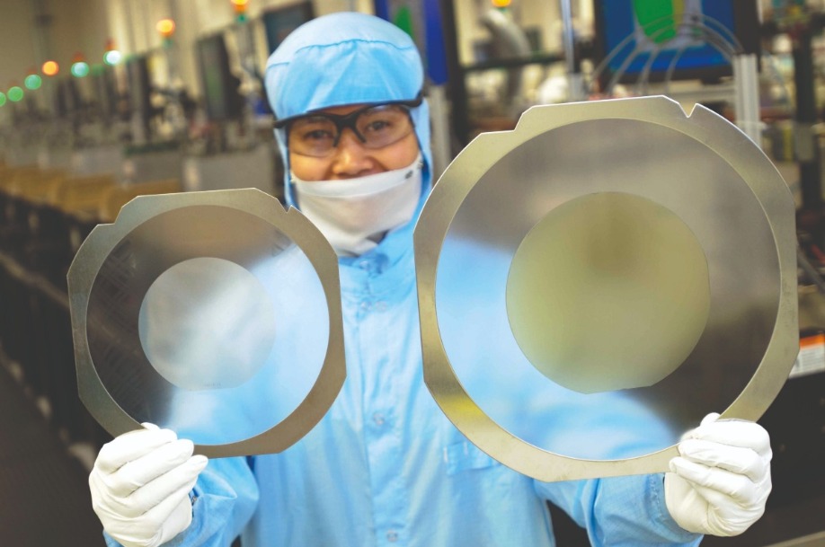
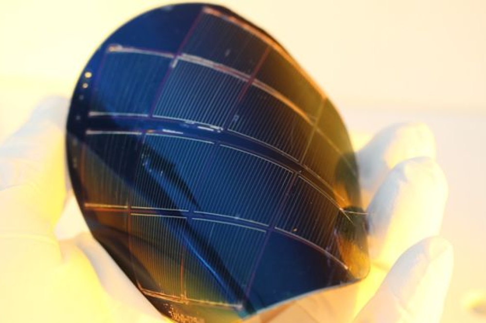
A Cree employee demonstrating the move from 100 mm to 150 mm SiC substrates.
Cree made much progress on all these fronts, introducing, in 2006, the industry’s first lighting-class LEDs. Known as the XLamp portfolio, these devices delivered 100 lumens per watt, exceeding the efficiency of fluorescent lighting. A revolution in lighting had started, after decades witnessing relatively little change.
LED lighting has many virtues. It’s robust, long-lasting, free from mercury, and its great efficiency trims electricity bills, in turn helping to reduce carbon footprints. But initially it did not find favour with the existing lighting infrastructure sector. That’s not that surprising, given the great business model of selling products to the public that could often fail within a year and had to be replaced. To drive a transformation, we started selling our own LED lighting fixtures to show the world what is possible. Our products consisted of a wide variety of indoor and outdoor lighting fixtures, ranging from fluorescent fixture replacements to LED streetlights.
Our final demonstration came in 2013, when we released our first LED light bulb. Rather than looking like something emerging from a science project, it had the style and feel of an incandescent bulb, and it retailed for less than $10. Launched to initiate the mass adoption of LED lighting, we called it ‘the biggest thing since the lightbulb.’
Following those major breakthroughs in LED lighting, we began putting additional emphasis in innovations outside the lighting space. This set us on a course for where we are today. Now our focus is to become a global semiconductor powerhouse that leads the transition from silicon to SiC.
Taking on the RF world
In 1998, we had our first major breakthrough in the RF domain, demonstrating the first GaN-on-SiC HEMT. Compared with the GaN-on-sapphire variants of the time, this device delivered increased signal gain and a 400 percent hike in power density in terms of watts per mm, making it an attractive candidate for wireless and broadcast high-power applications.

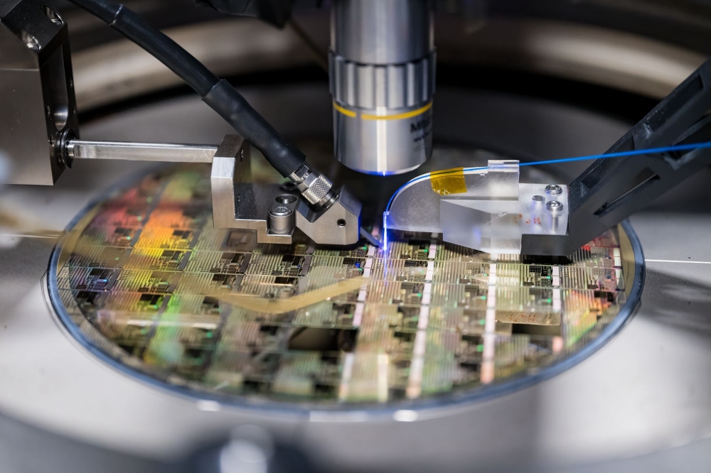
Cree employees examine product wafers.
Two years on, we demonstrated the first ever GaN MMIC. This device, producing a record power density, showcased the viability of this alternative to GaAs. The greatly superior power density of the GaN MMIC not only enables this device to support a higher power output – it could also serve much wider bandwidths for an equal power level.Further success came in 2008, when we introduced the first GaN RF device that utilised the benefits of GaN-on-SiC to improve RF performance. With its high breakdown field, GaN can operate at very high voltages, and thus high-power densities, without having to compromise reliability. By using SiC as the foundation, the GaN device sits on a very high-thermal-conductivity platform. This base is ideal for dissipating a high-power density and maintaining junction temperatures at a reasonable level. Thanks to this, GaN RF devices deliver higher output powers without having to increase device size. These attributes enable the RF industry to design smaller, more efficient, more powerful RF systems.
During the last decade, we have continued to advance the performance of our RF GaN-on-SiC devices. They are widely adopted by the aerospace and defence industries, which use them to improve the capabilities of their systems as well as in the telecom infrastructure market for higher-efficiency power amplifiers.
SiC powers up
Power electronics started coming of age at the beginning of the twentieth century. One of the earliest examples is the mercury-arc rectifier, developed in 1902 to convert AC power into a DC form. By the early 1930s, selenium had replaced mercury, only to be superseded by silicon in the 1950s. During that era engineers invented the first silicon BJTs and MOSFETs, but the latter would not become suitable for use in power electronics until the late 1970s. The last major breakthrough in silicon power electronics, the development of the IGBT, followed in the 1980s.
Within the power electronics world, the introduction of SiC provided the next big materials breakthrough. The US Army, Air Force, Navy, NASA and DARPA all supported these efforts, funding programs from the early 1990s. For SiC to establish itself as a mainstream technology, SiC wafers had to be cheaper, larger, and contain far fewer defects. Without a substantial fall in defect density, it would not be possible to produce devices with sufficient area to operate at high currents.
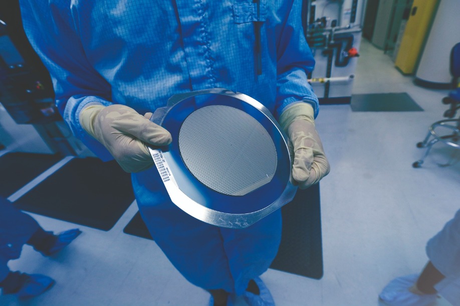
A up-close look at a 150 mm wafer in dicing.
A major impediment was the infamous micropipe defect. At one stage it was thought that micropipes were simply inherent to SiC, so impossible to eliminate. And that was not the only major stumbling block – oxides on SiC were considered to be inherently unreliable, preventing the manufacture of a reliable MOSFET. Even if both these daunting issues could be overcome, maybe that would be to no avail, if SiC wafers were never big enough to allow devices to serve in anything other than the most niche, cost-insensitive applications.
As history attests, all these issues have been addressed. Success on all fronts occurred after the launch of the first small SiC Schottky barrier diodes – introduced in 2001 and 2002 by Infineon and Cree, respectively – with progress paving the way to the introduction of first commercial SiC power MOSFET, which we launched in early 2011.
The introduction of SiC diodes and transistors has had a significant impact on the power electronics industry. It opened the door to faster switching frequencies, higher efficiencies, and superior power densities – all of which are key to the continued development of effective power electronic systems. These attributes allow SiC power electronics to support various emerging industries, including: renewable power conversion, such as solar energy and wind power; energy storage conversion; and electric trains, buses, and other types of public transportation.
SiC power devices can also be found in uninterruptible power supplies, industrial high-frequency power supplies, and motor drives. In all these applications, systems sporting SiC components operate with higher efficiencies take up less space, weigh less, and do not require extensive cooling systems. These valuable merits have taken us to a point where SiC is pushing the boundaries of innovation in a wide variety of industries.
An attitude of innovation
When we look back at these milestones over the past 25 years and think about all the breakthroughs in between, it is clear that Cree’s stubborn pursuit of innovation has been a driving force, both through the company’s history and that of SiC. There have been many obstacles, some considered insurmountable. It has led some to try and then give up, and others to never embark on these challenges.
There were those who argued that you cannot eliminate micropipes in SiC, that you can’t make a wafer larger than two inches, and that it’s impossible to make bipolar devices that don’t degrade. Cree has proved all those fallacies wrong due to a steadfast commitment to overcoming barriers. It is in our DNA that there is no reason to give up, just because someone says it can’t be done.
In some cases, we have not just broken barriers – we have kept on going, setting new benchmarks. After making the first 2 inch SiC substrate, we broke the 4-inch barrier, and now we’re ramping up 200 mm wafers, with mass production slated for the not too distant future. While it has certainly been a challenge and adventure to get this far, there is still so much more to come. As we look ahead, we see a future that has never been brighter. SiC is set to play an ever greater role in a variety of applications.
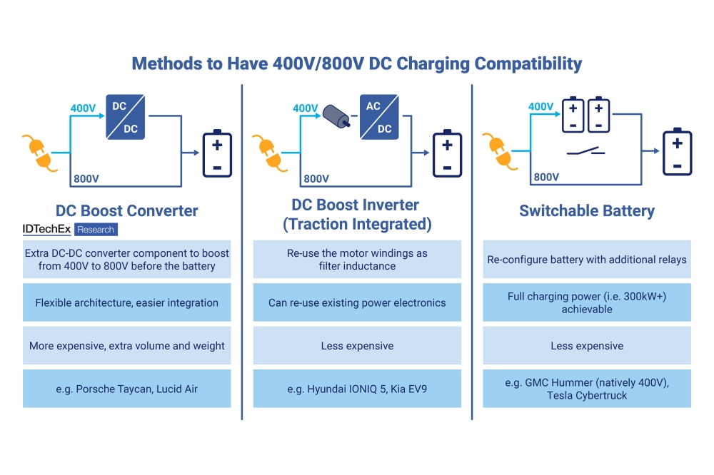
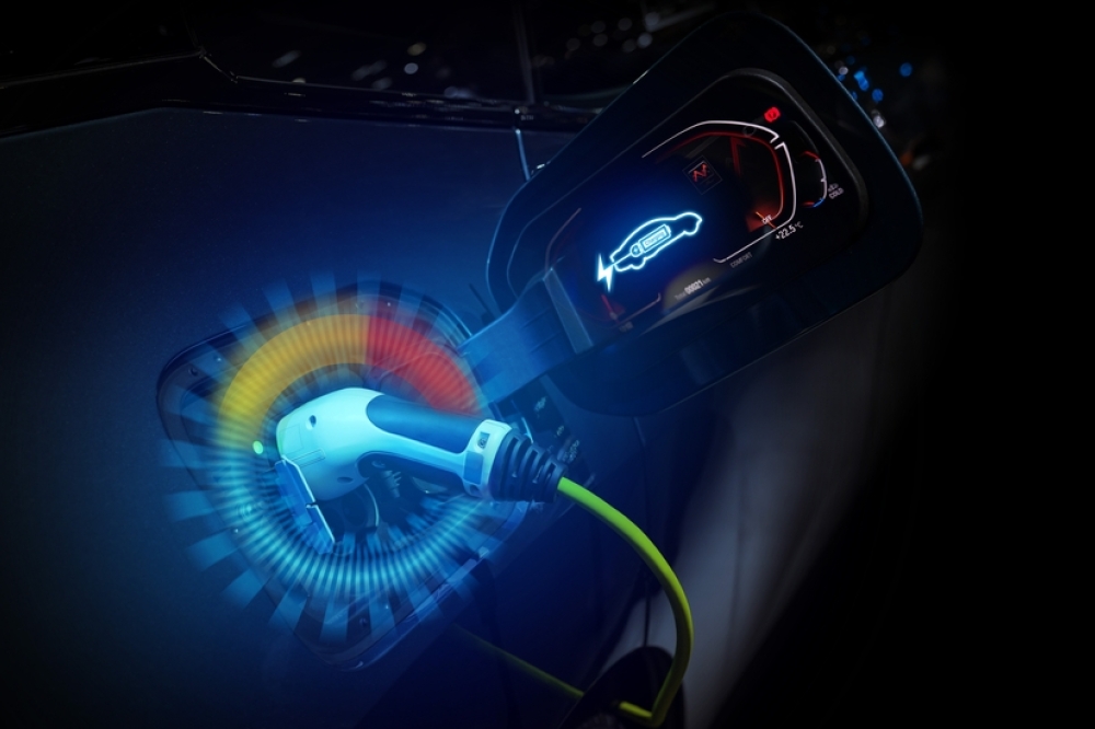
One of the biggest opportunities for SiC is in electric vehicles. Some of the first cars utilising this material are already on the road, and virtually every global manufacturer is including this technology in future designs that will grace the forecourts in the coming years. By replacing silicon devices with those made from SiC, the range of an electric vehicle can be extended by 5-10 percent, or the cost expended on expensive batteries trimmed by this amount. This most-welcome advantage is quickly positioning SiC as a necessary component in inverters as well as onboard and offboard chargers. As range is a significant factor for those considering the purchase of an electric vehicle, it has a tremendous influence on sales. And the use of SiC doesn’t always command a premium for electric-vehicle makers, as it can lead to an overall decrease in cost compared with the use of silicon technology. Its role looks set to grow further as electric vehicle manufacturers transition from 400 V to 800 V systems, which get an even bigger benefit from the switch to SiC, in terms of efficiency and other measures of performance.

Throughout the last 25 years there has been rapid innovation within the communications sector. It is currently undergoing a proliferation of 5G networks and picocells as well as higher volumes of small distributed antennas, radar applications, aerospace and defence tools. For all these applications,
GaN-on-SiC devices have the edge over silicon in efficiency and bandwidth, while offering a far smaller footprint. Drawing on the advances wrought by SiC has increased demand for this material. To bolster global supply, of which we account for 60 percent, we have committed to a $1 billion expansion at our Durham headquarters as well as the construction of an additional manufacturing facility in the Mohawk Valley, New York. When this additional production is available, our company’s capacity will have increased 30-fold from its level in 2017.
In the past 25 years, there has been more change in the SiC and semiconductor industries than we could ever have imagined. Looking ahead, the next 25 years are shaping up to be even more transformational. We expect that they will deliver breakthroughs that seem impossible today. It is an exciting time to participate in these changes, while looking forward to ground-breaking times that lie ahead.