Kyma updates progress on AlGaN and AlN development
Kyma Technologies, a supplier of crystalline nitride semiconductor materials, has provided an update on its progress in crystalline AlGaN and AlN materials development and to state its desire to collaborate with bulk AlN developers interested in improving the optical transparency of their materials.
Kyma has over a decade of experience in the fabrication of AlN templates which are thin films of crystalline AlN deposited on sapphire, silicon, or SiC substrates. The process uses Kyma’s patented and proprietary III-N Plasma Vapour Deposition of NanoColumns (PVDNC) technology.
These products are gaining acceptance with customers engaged in blue and green LED manufacturing. The nanocolumnar nature of Kyma’s PVDNC AlN templates present an excellent surface for nucleating GaN buffer layers which then can be followed by a high quality GaN LED device structure.
Recently Kyma began extending its process capabilities to develop materials which are designed to support high Al content device layer structures. Such structures are of interest for UV and high temperature and high power electronics applications.
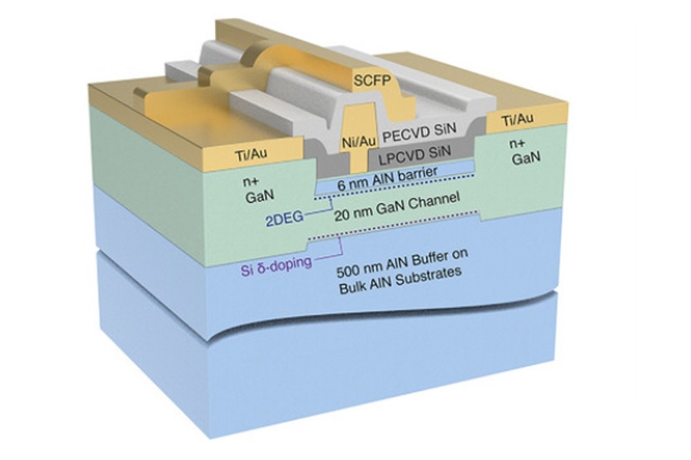
Keith Evans, Kyma’s president & CEO, stated: “While our PVDNC AlN templates are excellent substrates for manufacturing GaN-rich devices such as blue and green LEDs and AlGaN/GaN field effect transistors (FETs), we are also employing other processes to develop materials that are specifically tailored to support the manufacturing of AlN-rich devices such as mid UV LEDs for germicidal irradiation and AlN/AlGaN FETs for temperature insensitive high power electronics applications.”
Towards these goals, Kyma is exploring and has made significant progress in the growth of crystalline AlN and AlGaN materials using high growth rate hydride vapour phase epitaxy (HVPE).
By adding a novel Al source to their HVPE tools, Kyma is now able to grow crystalline AlN and a broad range of AlGaN compositions. And just like GaN HVPE, the structural quality of the HVPE grown AlN and AlGaN crystals are influenced by the seed crystal that they are grown upon.
Kyma has already demonstrated the ability to deposit crystalline AlN by HVPE on a range of starting seed materials, including on AlN structures which were produced by other techniques.
Ed Preble, Kyma’s CTO & VP business development, stated, “Our AlN HVPE process appears to have many of the traits of our GaN HVPE process. We are able to rapidly replicate the quality of the underlying seed and in certain cases then improve its quality as we continue to grow the crystal.”
“Additionally, optical transmission measurements show that our HVPE grown AlN materials have high transparency in the 200nm to 400nm spectral region, an important feature for UV LED applications, and a noted advantage over some competing AlN crystal growth approaches,” added Preble.

