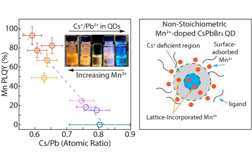
Fast method for printing nanolasers from perovskites
An international research team has developed a new method of synthesising miniature light sources. It is based on a special laser which produces millions of nanolasers from a perovskite film in a few minutes. Such lasers look like small disks, work at room temperature and have an tunable emission wavelength from 550 to 800 nm. The high speed and good reproducibility of this method make it promising for the industrial production of single nanolasers as well as whole chains. The study was published in ACS Nano.
Recently, scientists have been actively working on miniature light sources or nanolasers. It is required, for example, to produce optical chips that could process information in next-gen devices. However, making such light sources is not that easy due to unstable materials, as well as the complex and expensive fabrication methods, which are difficult to control and adjust for industrial production.
Scientists from ITMO University, the Far Eastern Federal University, Texas University at Dallas, and the Australian National University have found a new way to solve this problem. They have developed a method allowing for creation of millions of nanolasers from an optically active halide perovskites in a few minutes.
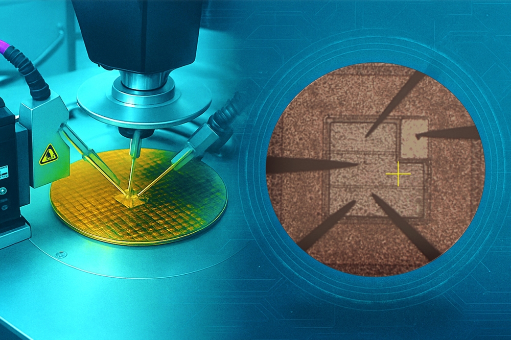
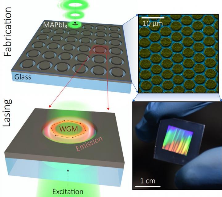
The fabrication starts when a half of micron thick perovskite film is deposited on a glass substrate. Then, it is irradiated with a laser beam with a special annular pulse intensity distribution: weak in the center and stronger at the edges. As a result, a set of perovskite disks is obtained from the film. These are the nanolasers: they are located on the substrate at an equal distance from each other, and have the same size and emission characteristics.
"Such perovskite disks, unlike regular film, act as so-called 'whispering gallery' resonators. The spontaneously emitted light in them can be traped, enhanced, and converted to coherent light. It is very important that we were able to create nanolasers that operate at the same wavelength. Their rough surface supress all the modes, except one, for which the lasing conditions are most suitable. At the same time, we can control the radiation wavelength by varying the composition of the film," says Sergey Makarov, the head of the Laboratory for Hybrid Nanophotonics and Optoelectronics at ITMO University.
Previously, scientists from ITMO University have proposed a chemical method for creating perovskite nanolasers. It helped to speed up the process but did not give enough control over the synthesis. Therefore, among the main advantages of this new method are not only high speed but also good 'controllability'. This makes it promising for industrial adaptation. Researchers currently plan to optimize the fabrication of nanolasers for industrial production and integrate nanolasers with waveguides to create optical chips.