ASM AMICRA Unveils three new manufacturing systems

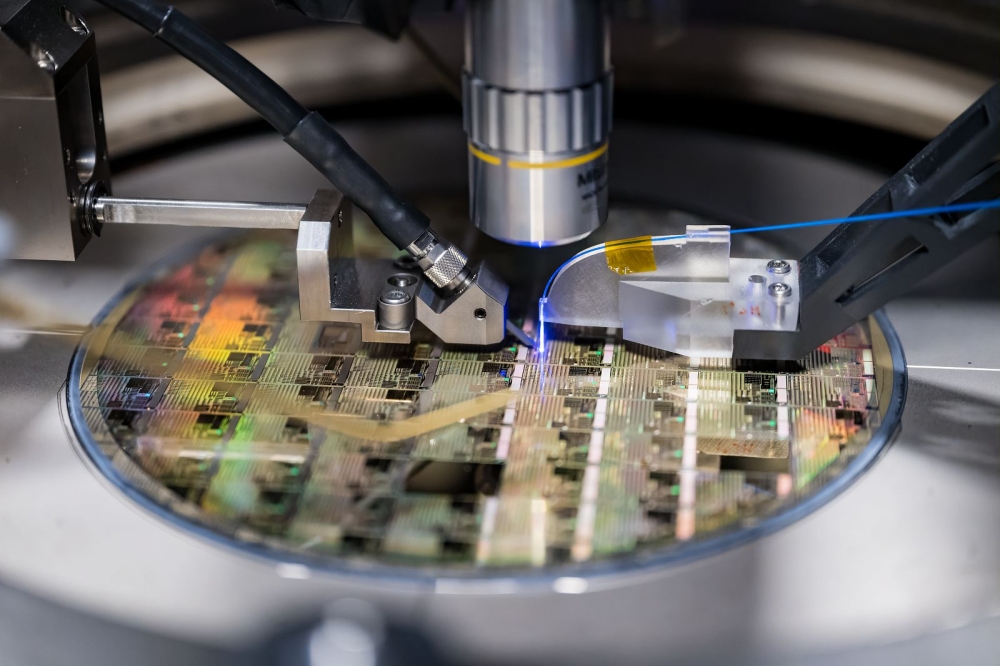
ASM AMICRA Microtechnologies GmbH (“ASM AMICRA”) has announced three new manufacturing systems that combine X-Celeprint’s Micro-Transfer Printing (MTP) and ASM AMICRA’s high precision die bonding technology to introduce the complete system to enable high volume heterogeneous integration of ultra-thin dies onto up to 300mm base wafers.
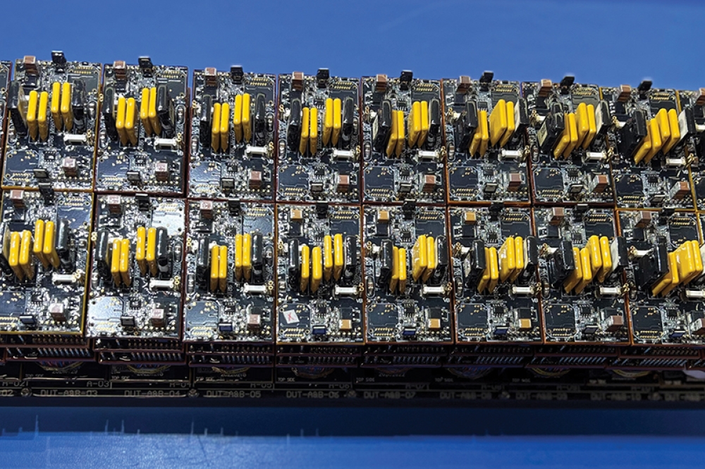
X-Celeprint’s MTP process stacks ultra-thin dies known as ‘x-chips’, which can be extremely varied[1] and made using very different process nodes and technologies[2], to create virtually monolithic 3D ICs that improve power, performance, area, cost, time-to-market and security for a wide array of applications including high-performance computing, communications, mobile, automotive, industrial, medical, or defense systems.
ASM AMICRA has been perfecting ultra-high precision placement technology for almost 20 years, and has now incorporated X-Celeprint’s MTP technology into three different manufacturing systems. These are:
The Nova+ MTP system, which serves high throughput needs with a fully automatic ISO 4 clean room class system using a 50x50mm MTP stamp enabling massively parallel pick-and-place of x-chips. Placement accuracy is +/- 1.5-microns with a 40-second cycle time.
The NANO MTP system, which serves markets such as photonics that require more precise placement accuracy (plus-or-minus 0.3-microns).
The AFC+ MTP system, which serves R&D and low volume manufacturing markets. Placement accuracy is plus-or-minus 1.0-microns with a 50-second cycle time.
X-Celeprint and ASM AMICRA are facilitating the adoption of MTP technology through development support, including design consultation with assistance in optimizing design and processes and prototyping services to ensure successful product launches. An extensive network of suppliers, manufacturers, and researchers are available to support customer project needs, including licensing programs.
“This agreement with X-Celeprint brings revolutionary technology to market for photonics and 3D heterogeneous integration,” said Dr. Johann Weinhändler, Managing Director, ASM AMICRA Microtechnologies GmbH. “MTP technology offers efficient handling of high volumes of large arrays of ultra-thin, brittle dies, as well as the ability to integrate dies from several different source wafers. MTP technology will provide semiconductor manufacturers with a critical, additional ‘tool in the toolbox’ that supplements conventional and advanced packaging technology.”
“The ultra-high precision capabilities of ASM AMICRA’s MTP manufacturing systems for heterogeneous integration of large arrays of ultra-thin x-chips has the potential to be a game-changer for semiconductor manufacturers seeking to extend Moore’s Law with 3D IC heterogeneous integration,” said Kyle Benkendorfer, X-Celeprint’s CEO. “Enabling chip designers to combine the optimum materials and different process technologies in 3D ICs results in more powerful devices, with higher density, increased functionality, lower cost, higher yield, and faster time to market.”


